Pioneering advances in semiconductor design for sensing light beyond the visible
Potential of thin-film-based image sensors unlocked with the integration of a pinned-photodiode structure
In short
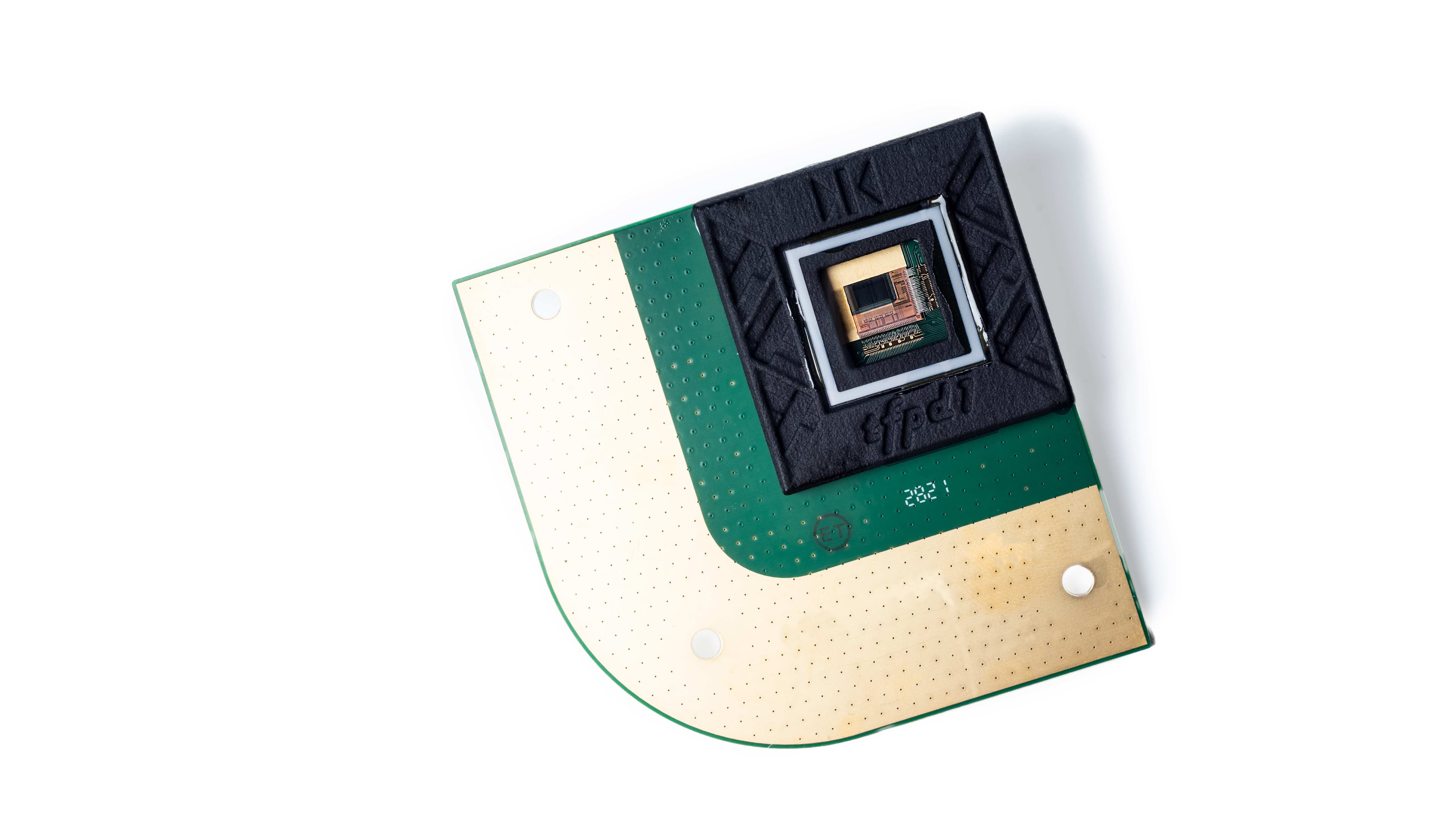
For the first time, researchers from imec succeeded in integrating a pinned photodiode structure in thin-film image sensors.
With the addition of a pinned-photogate and a transfer gate, the superior absorption qualities of thin-film imagers -beyond one µm wavelength- can finally be exploited, unlocking the potential of sensing light beyond the visible in a cost-efficient way.
This novel approach opens doors to diverse applications, from autonomous driving to environmental monitoring.
This article appeared earlier in Laser Focus World.
Overcoming silicon’s limits
Silicon-based imagers excel at capturing visible light. However, for longer wavelengths such as (short-wave) infrared (SWIR or IR), offering applications ranging from a camera supporting the sorting of household waste to autonomous vehicles 'seeing' through smoke or fog, alternative semiconductors are necessary.
While III-V materials are addressing this need, their high manufacturing costs limit their widespread use, crucial for large-scale roll-out in domains like automotive. Enter the promising alternative of thin-film-based absorbers, including organic compounds or quantum dots. These materials feature superior absorption characteristics and can be more easily integrated with conventional CMOS readout circuits.
Breaking barriers with pinned photodiode structures
Nonetheless, the adoption of infrared sensors utilizing thin-film absorbers faces challenges, primarily related to low signal-to-noise ratios leading to poor image quality. Recent developments have overcome these issues for the first time. Not by changing the choice of materials, but by building on the rich history of pinned photodiode (PPD) structures in silicon-CMOS image sensors, dating back to the 1980s.
The PPD structure, with its additional transistor gate and specialized photodetector structure (termed photogate), significantly reduces noise, making it a dominant force in the consumer market for silicon-based image sensors. It allows reset operation of the transistor without kTC noise nor the effect of the previous frame, providing a kind of ‘super-switch’ by which charges can be completely drained. However, incorporation of a PPD in thin-film-based sensors has never been possible because of the complexity of integrating two different semiconductor systems.
A leap in image sensor architecture
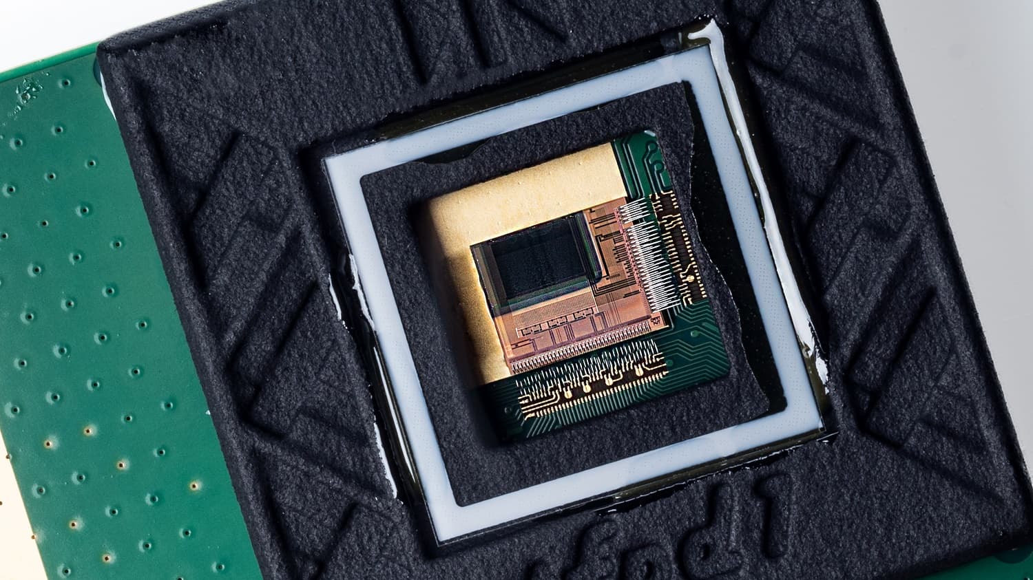
In a recent Nature Electronics paper, researchers from imec presented the successful incorporation of a PPD structure in the read-out circuitry of a thin-film pixel. The proof-of-concept leverages imec’s in-house expertise in both thin-film materials and photodiodes, surpassing current thin-film pixel architectural limitations. While the individual components of this pixel have been around for a long time and have proven their worth in other applications, this proof of concept demonstrates their collective value and versatility in sensing light beyond visible.
For the photogate transistor, indium-gallium-zinc-oxide (IGZO) was used, due to its compatibility with thin-film photodiodes and because it can be integrated into silicon read-out circuits. Such transistors have already demonstrated their effectiveness in various applications, including memory technologies.
Next, this IGZO transistor was monolithically hybridized with a thin-film organic photodiode directly on top of the complementary metal-oxide semiconductor (CMOS) readout circuitry. This wafer-level post-processing enables scalable and affordable manufacturing, paving the way for large-scale applications.
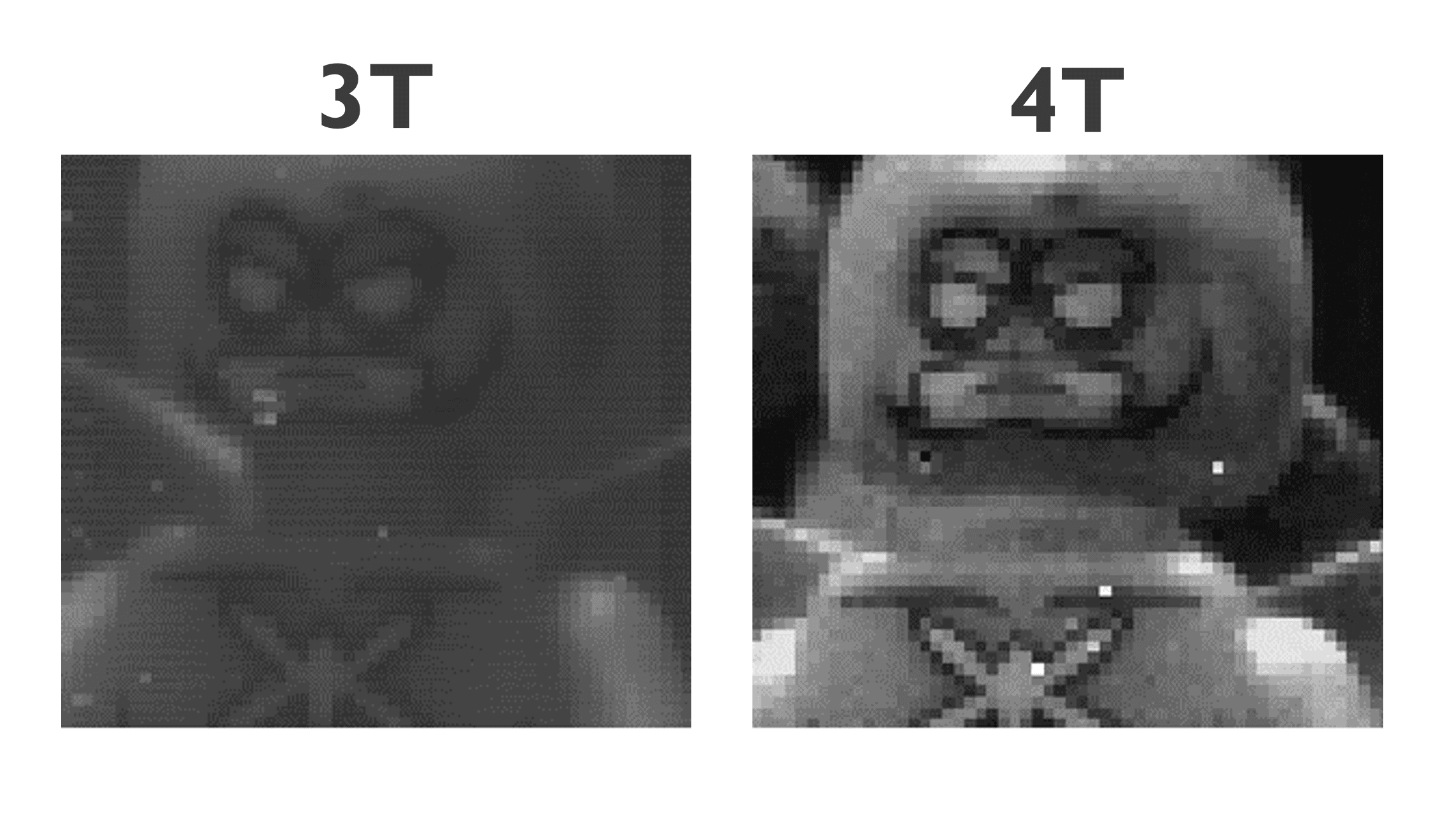
The resulting 4T SWIR imager showed a low read-out noise of 6.1e-, compared to >100e- for the conventional 3T reference sensor. With such a reduction in noise, higher signal-to-noise ratios (SNR) can be achieved. As a result, images can be captured with more accuracy and detail. Moreover, as fewer photons are necessary to induce signals, even weak signals can be converted into images.
Advancements in linearity: the key to precision
In follow-up research, the team showed that the introduction of this PPD pixel structure also resulted in a more linear response – a measure for the accuracy of image reproduction. Moreover, the photodiode bias was fixed, effectively reducing dark current (by 72%) and increasing the linearity (error reduction of 59%) for organic thin-film photodiode-based image sensors. Thus, adding a photogate ensured a more faithful representation of the captured scene, critical for applications where accurate image reproduction is paramount.
In addition to this, the initial pixel was designed to maximize charge to voltage conversion gain – with a resulting limited floating diffusion capacitance – thus not able to demonstrate high full-well capacity. A second-generation pixel structure did enable a high full-well capacity exceeding 1 Mega electrons of the proposed pixel (with a pitch of 5 µm). This ensures a dynamic range of > 100 dB, compared to the 82 dB of the 3T pixel, representing the ability of this high SNR pixel to capture a wide range of light intensities – from the darkest to the brightest.
Future horizons: accelerating thin-film-based image sensor deployment
This pixel architecture offers opportunities for other promising thin-film photodiodes beyond organic, including perovskite absorbers or quantum dots. Since the photodiode is separated from the readout circuit and integrated via post-processing, the used absorption materials do not need to undergo stringent optimization before integration with the readout circuitry. This novel 4T pixel architecture can accelerate the deployment of monolithic thin-film-based image sensors. The benefits of this new architecture could serve as a catalyst for novel applications that are either not covered or inadequately addressed by silicon imagers.
Explore the peer-reviewed studies underpinning this article:
- J. Lee et al., Nat. Electron., 6, 590–598 (2023); https://doi.org/10.1038/s41928-023-01016-9.
- J. H. Kim et al., Sensors, 23, 8803 (2023); https://doi.org/10.3390/s23218803.
- M. Jin et al., IEEE Electr. Device L., 44, 12, 2007–2010 (Dec. 2023); https://doi.org/10.1109/led.2023.3325830.
Authors

Pawel Malinowski
Pawel E. Malinowski obtained his MSc in electronics and telecommunications, specializing in radiation-tolerant integrated circuits, from Lodz University of Technology, Poland, in 2006. He completed his Ph.D. in electrical engineering at KU Leuven, Belgium, in 2011, focusing on III-nitride-based imagers for space applications. Since 2011, he has been a senior researcher and program manager in the Sensor and Actuator Technologies Department at imec.
His research spans emerging photodetectors, image sensors, and high-resolution OLED displays. Pawel has authored/co-authored over 80 publications and received awards including the International Display Workshops Best Paper Award in 2014 and the SID Display Week 2018 Distinguished Paper Award.

Jiwon Lee
prof. Jiwon Lee earned a Ph.D. degree in 2013 from the Department of Electrical Engineering at the Korea Advanced Institute of Science and Technology (KAIST), South Korea. Following this, he worked as a senior researcher at Samsung Electronics. Starting in 2018, he served as the Principal Member of Technical Staff at imec. In 2022, he transitioned to become an associate professor in the Department of Photonics and Nanoelectronics at Hanyang University (ERICA Campus), where he currently holds the position of assistant professor in the Department of Semiconductor Engineering. Additionally, since 2023, he has served as a guest professor at imec, focusing on topics related to novel image sensors. His research interests encompass the development of innovative image sensor pixels for various applications.

Nikolas Papadopoulos
Nikolas P. Papadopoulos received his MSc in Electrical and Computer Engineering in 2005 and completed his Ph.D. in poly-TFT circuit design at Aristotle Univ. Thessaloniki in 2010, including an ERASMUS scholarship at UPC, Spain, focusing on solution processed TFTs and circuits. After that, he served as a postdoc and research associate with the AFET group at the Univ. of Waterloo, Canada, concentrating on CMOS driving, monitoring, and TFT circuit designs for AMOLED displays. Joining imec in 2015, he specialized in (analog) circuits and RFID/NFC tags on plastic substrates for various publicly funded projects. Since 2022, Nikolas has been serving as a senior researcher and technical lead of TFT circuit design at imec, spearheading the Thin-Film PPD project.
Nikolas has contributed to the FP7 project PYTHAGORAS and various H2020 projects, including CAPID, A-PATCH, FLICS, PING (EU innovation award winner), Hi-Response, and SMARTEES. With over 70 peer-reviewed publications in prestigious journals such as Nature, IEEE, and SID, his research was showcased on the cover of Nature Electronics in 2019.