Imec integrates thin-film pinned photodiode into superior short-wave-infrared imaging sensors
Results published in Nature Electronics unlock the potential of thin-film sensors in infrared imaging
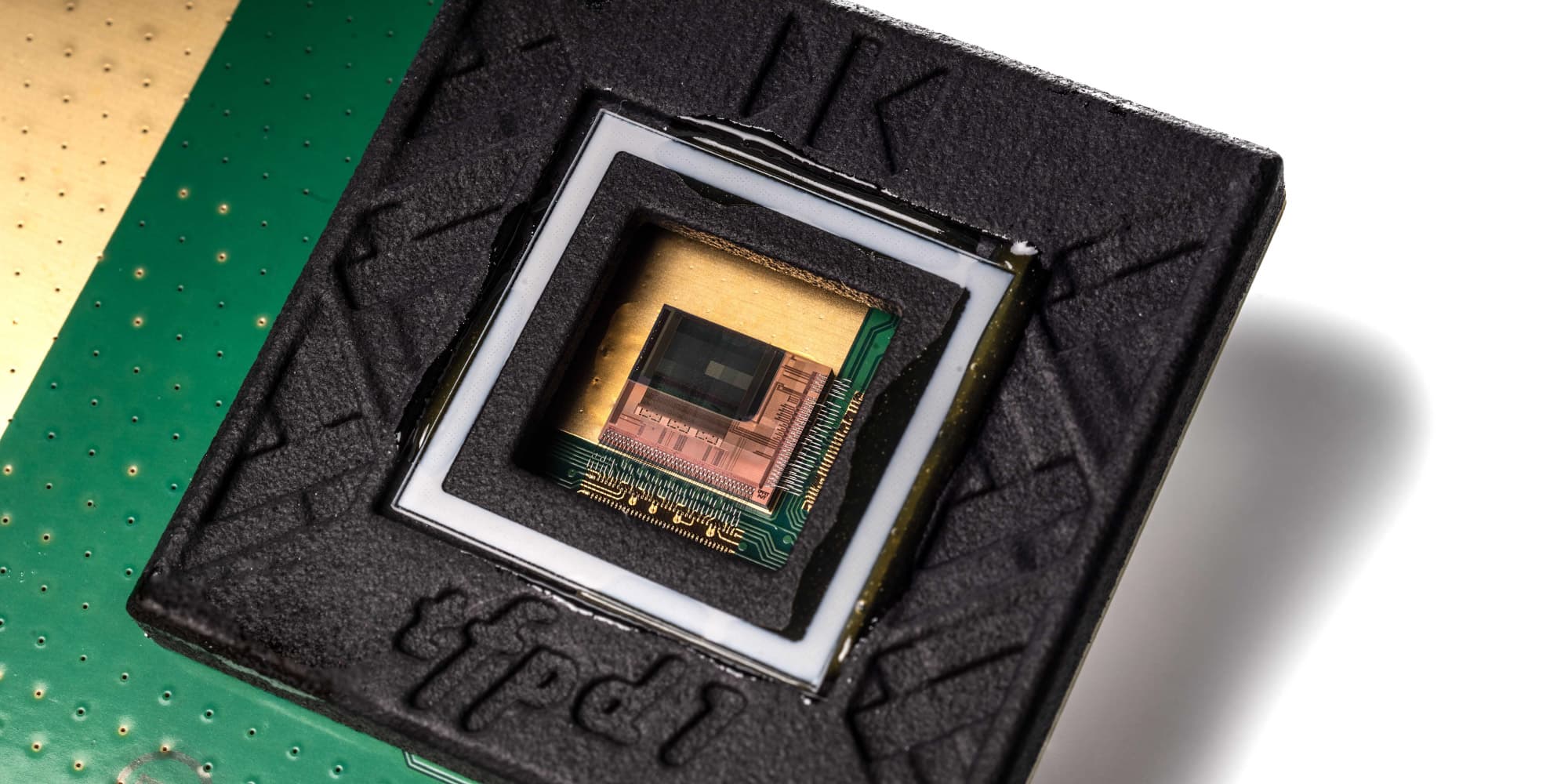
LEUVEN (Belgium), 14 August, 2023—Imec, a world-leading research and innovation hub in nanoelectronics and digital technologies, presents the successful integration of a pinned photodiode structure in thin-film image sensors. With the addition of a pinned-photogate and a transfer gate, the superior absorption qualities of thin-film imagers -beyond one µm wavelength- can finally be exploited, unlocking the potential of sensing light beyond the visible in a cost-efficient way.
Detecting wavelengths beyond visible light, for instance infrared light, offers clear advantages. Applications include cameras in autonomous vehicles to ‘see’ through smoke or fog and cameras to unlock your smartphone via face recognition. Whilst visible light can be detected via silicon-based imagers, other semiconductors are necessary for longer wavelengths, such as short-wave infrared (SWIR).
Use of III-V materials can overcome this detection limitation. However, manufacturing these absorbers is expensive, limiting their use. In contrast, sensors using thin-film absorbers (such as quantum dots) have recently emerged as a promising alternative. They have superior absorption characteristics and potential for integration with conventional (CMOS) readout circuits. Nonetheless, such infrared sensors have an inferior noise performance, which leads to poorer image quality.
Already in the 1980’s, the pinned photodiode (PPD) structure was introduced for silicon-CMOS image sensors. This structure introduces an additional transistor gate and a special photodetector structure, by which the charges can be completely drained before integration begins (allowing reset operation without kTC noise nor the effect of the previous frame). Consequently, because of lower noise and improved power performance, PPDs dominate the consumer market for silicon-based image sensors. Beyond silicon imaging, incorporating this structure was not possible up until now because of the difficulty of hybridizing two different semiconductor systems.
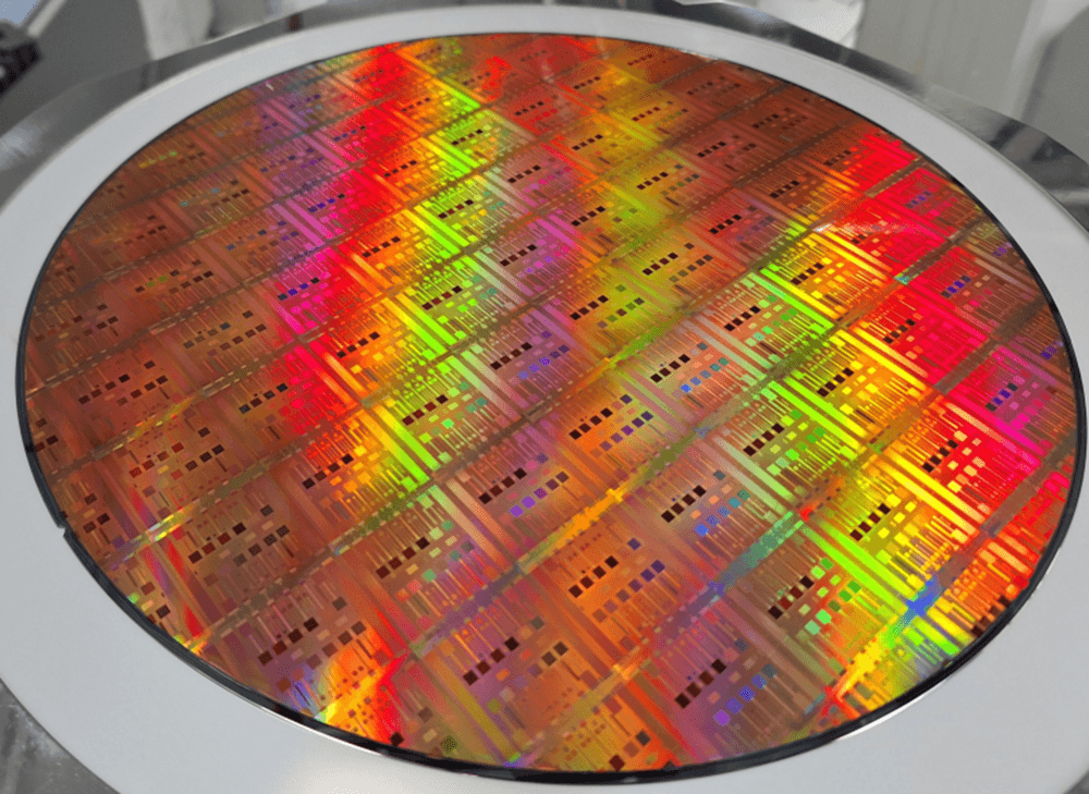
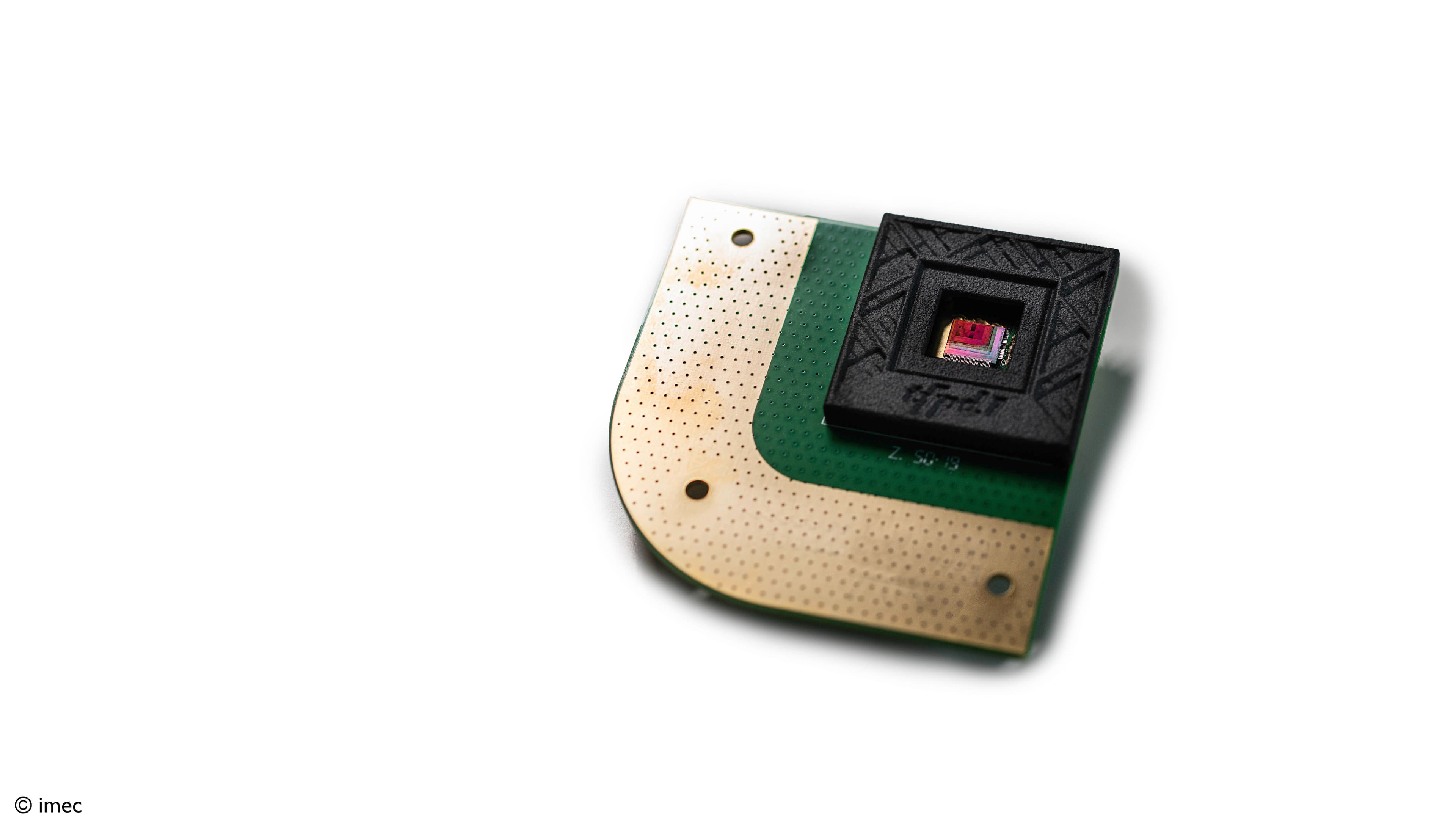
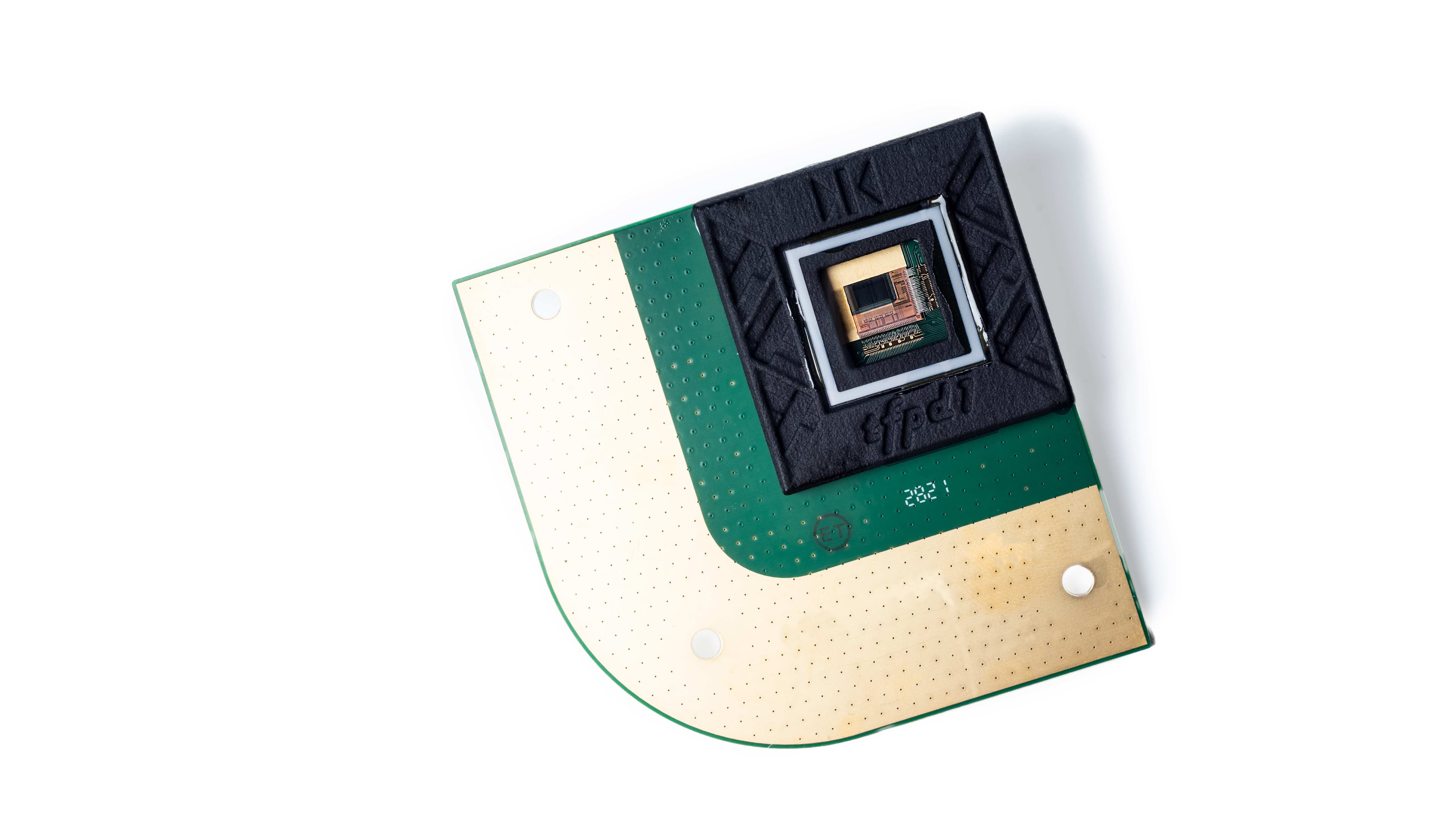
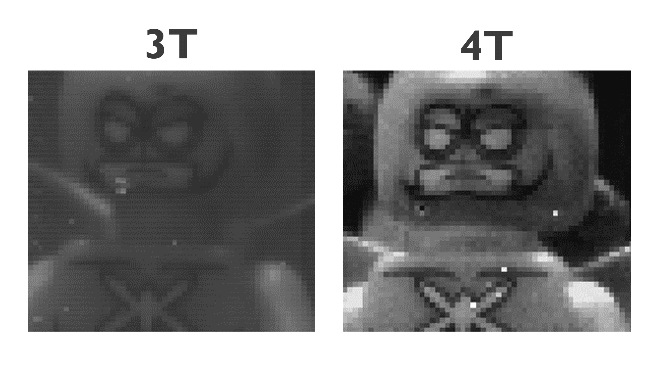
Now, imec demonstrates successful incorporation of a PPD structure in the readout circuit of thin-film-based image sensors; the first of its kind. A SWIR quantum-dot photodetector was monolithically hybridized with an indium-gallium-zinc oxide (IGZO)-based thin-film transistor into a PPD pixel. This array was subsequently processed on a CMOS readout circuit to form a superior thin-film SWIR image sensor. “The prototype 4T image sensor showed a remarkable low read-out noise of 6.1e-, compared to >100e- for the conventional 3T sensor, demonstrating its superior noise performance” stated Nikolas Papadopoulos, project leader ‘Thin-Film Pinned Photodiode’ at imec. As a result, infrared images can be captured with less noise, distortion or interference, and more accuracy and detail.
Pawel Malinowski, imec Program Manager ‘Pixel Innovations’ adds: “At imec, we are at the forefront of bridging the worlds of infrared and imagers, thanks to our combined expertise in thin-film photodiodes, IGZO, image sensors and thin-film transistors. By achieving this milestone, we surpassed current pixel architectural limitations and demonstrated a way to combine the best performing quantum-dot SWIR pixel with affordable manufacturing. Future steps include optimization of this technology in diverse types of thin-film photodiodes, as well as broadening its application in sensors beyond silicon imaging. We are looking forward to further these innovations in collaborations with industry partners.”
The findings are published in the August 2023 edition of Nature Electronics "Thin-film image sensors with a pinned photodiode structure". Initial results were presented at the 2023 edition of the International Image Sensors Workshop.
About imec
Imec is a world-leading research and innovation center in nanoelectronics and digital technologies. Imec leverages its state-of-the-art R&D infrastructure and its team of more than 5,500 employees and top researchers, for R&D in advanced semiconductor and system scaling, silicon photonics, artificial intelligence, beyond 5G communications and sensing technologies, and in application domains such as health and life sciences, mobility, industry 4.0, agrofood, smart cities, sustainable energy, education, … Imec unites world-industry leaders across the semiconductor value chain, Flanders-based and international tech, pharma, medical and ICT companies, start-ups, and academia and knowledge centers. Imec is headquartered in Leuven (Belgium), and has research sites across Belgium, in the Netherlands, and representation in 3 continents. In 2022, imec's revenue (P&L) totaled 846 million euro.
Further information on imec can be found at www.imec-int.com.
Imec is a registered trademark for the activities of imec International (IMEC International, a legal entity set up under Belgian law as a “stichting van openbaar nut”), imec Belgium (IMEC vzw supported by the Flemish Government), imec the Netherlands (Stichting IMEC Nederland), imec Taiwan (IMEC Taiwan Co.), imec India (IMEC India Private Limited), imec San Francisco (IMEC Inc.) and imec Florida (IMEC USA Nanoelectronics Design Center Inc.).