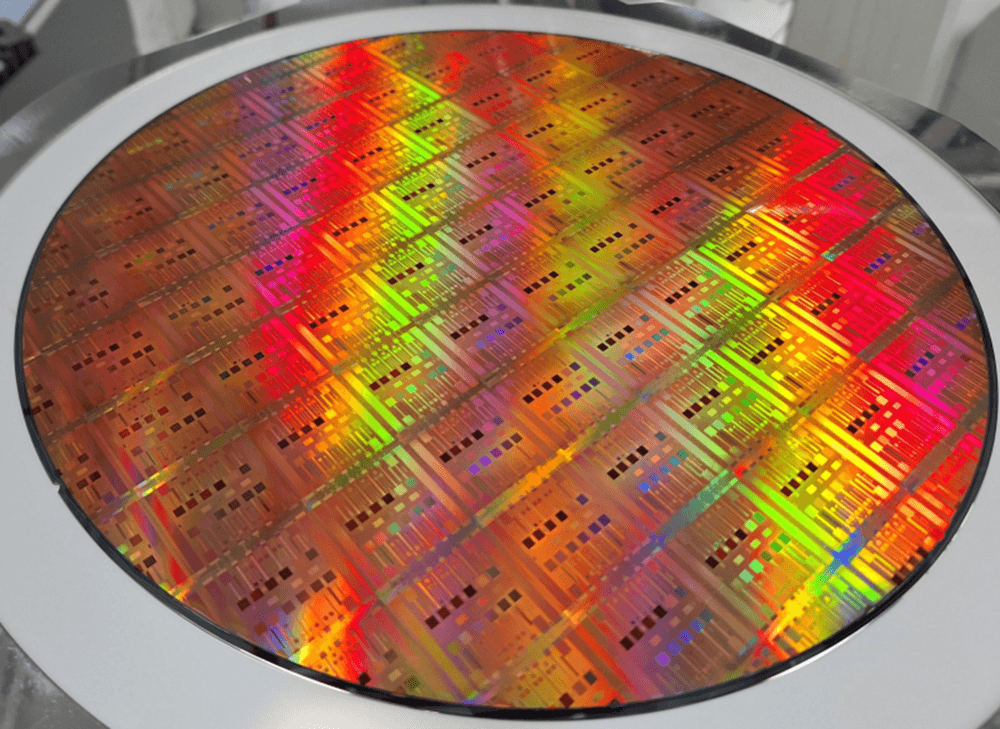
Nanowell field-effect transistor for highly sensitive molecular detection
Towards scalable single-molecule sensing for genomics and proteomics
In short
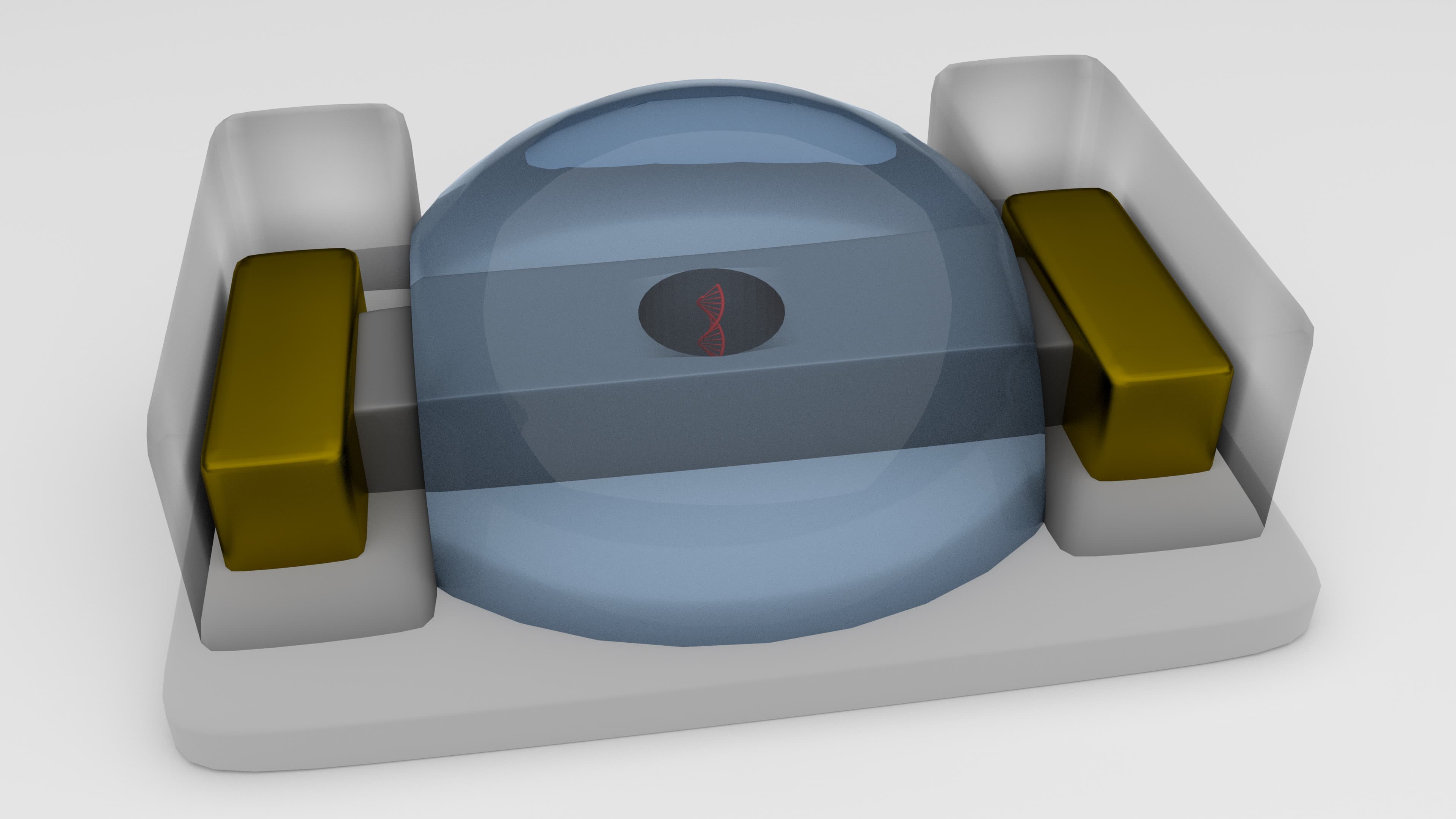
Researchers at imec unveil a pioneering bio-molecular sensor device – a nanowell FET, an upgraded version of their earlier FinFET biosensor.
The device features a 25 nm size nanowell in the center of a 35-40 nm wide silicon FinFET, enhancing molecular detection sensitivity, with near-ideal electrical properties.
Additionally, binding inside the nanowell may become self-limiting, which could enable single-molecule sensing.
The landscape of single-molecule sensing
Since the Human Genome Project's monumental feat of the first sequenced human genome in 2003, high-throughput sequencing has witnessed remarkable advancements. The pivotal role of DNA testing and sequencing came to the forefront during the COVID-19 pandemic, where it played a crucial role in diagnostic testing and understanding the SARS-CoV-2 virus. Next to this, the cost of DNA screening, once a staggering $100 million, has plummeted to $1,000, opening avenues for cost-effective applications like Non-Invasive Prenatal Testing (NIPT).
Challenges in short-read sequencing technologies arise from the need for amplification of the initial sample and synchronization of identical molecules, limiting identification to no more than 300 base pairs at a time. However, single-molecule sensing could provide a solution by eliminating the need for this amplification. What is more, highly efficient reading technologies could facilitate the use of DNA as archival data storage, which is currently a very costly endeavor. Research in life sciences therefore remains on the lookout for platforms that can offer fast and cost-effective single molecule sensing solutions, including not only DNA but also other molecules.
Proteins, for instance, are a cornerstone in medical diagnostics due to their direct correlation with an individual's phenotype. The dynamic proteome, which consists of millions of proteins, offers remarkable specificity for diseases compared to our static genome of around twenty thousand genes. However, it poses unique reading challenges. Proteins, with their twenty different amino acids as building blocks, cannot be replicated and plasma concentration levels can span between sixteen orders of magnitude. High-throughput single-molecule sensing therefore becomes imperative, especially for conditions where low-prevalent proteins are of interest, such as early-stage cancer.
Enter chip-based life sciences
Chip-based life sciences applications, combining biosensing or sequencing with the semiconductor industry's prowess in nanoscale devices, have the potential to revolutionize our understanding of biology. Nonetheless, its applications in e.g., genome and proteome sequencing remain largely in development.
Notable examples of single-molecule sensing currently on the market include zero mode waveguides and nanopores. While these offer significant advantages to short-read technologies, challenges like optical diffraction and limited throughput persist, making them relatively bulky or limited in output, respectively.
Imec's innovative approach
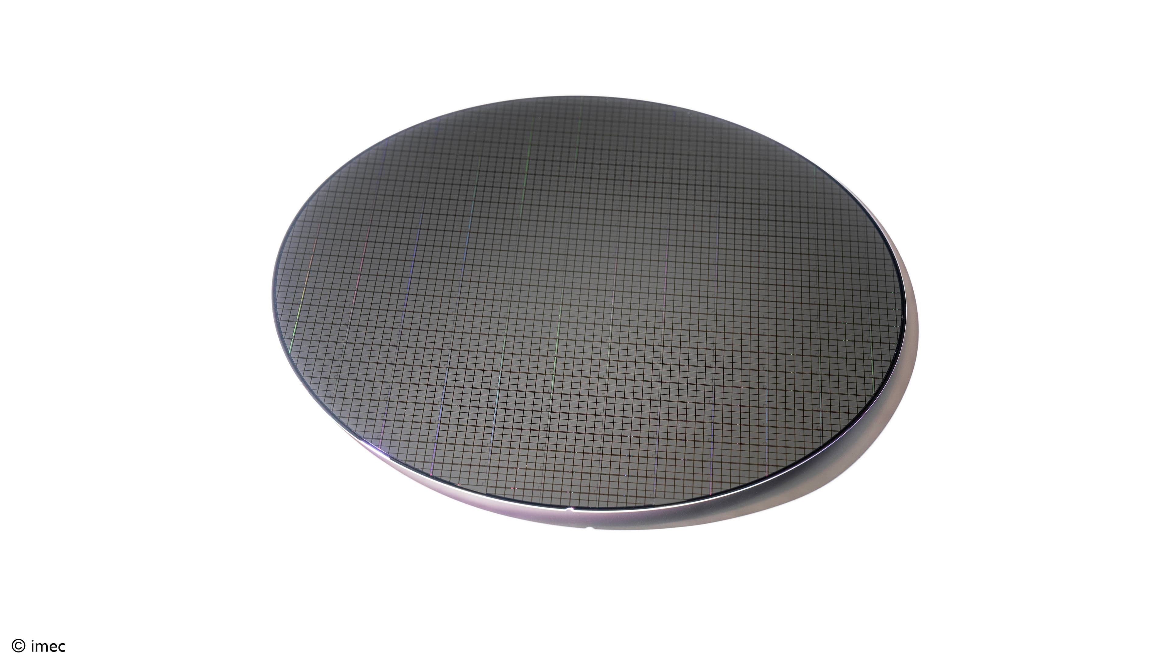
To address these challenges, imec is leveraging its CMOS technology and 300 mm cleanroom towards the electrical realization of biochemical sensors. Moving away from conventional optical approaches, the read-out circuitry is directly incorporated into the biosensor, enabling faster processing. Moreover, with billions of transistors fitting onto a chip, unprecedented parallelization can be realized. This could pave the way to high-throughput sensing platforms for e.g., DNA detection, greatly surpassing the throughput of those currently available, or for protein detection, currently non-existent.
More specifically, imec is researching the modification of traditional metal oxide semiconductor field-effect transistors (MOSFETs) into liquid gated field-effect transistors. The resulting device gives a measurable ‘switch’ electrical signal when biomolecules attach to the chemically modified dielectric surface of the gate, leading to a change in its threshold voltage. For such liquid-gated FETs, or CMOS compatible biosensors, the width and length of the ‘nanowire’ gates are ideally scaled down to tens of nanometers (any smaller and the signal saturates and eventually drops), to optimize single-molecule sensing. This enhances sensitivity, since the single-molecule signal of a transistor is reversely proportional to the surface, which is true to a lesser extent for its noise.
Obtaining well-performing nanoscale CMOS devices in liquid environments is challenging. This is partly because inversely charged ions in the liquid environment are attracted to charged biomolecules, screening the charge intended for detection (and therefore termed ‘charge screening’).
In 2020, imec achieved a breakthrough by addressing these challenges. The result: the smallest silicon FinFET-based biosensor, with an unprecedented 50 nm long channel and capable of detecting minuscule amounts of DNA molecules.
Nanowell FET: a new chapter
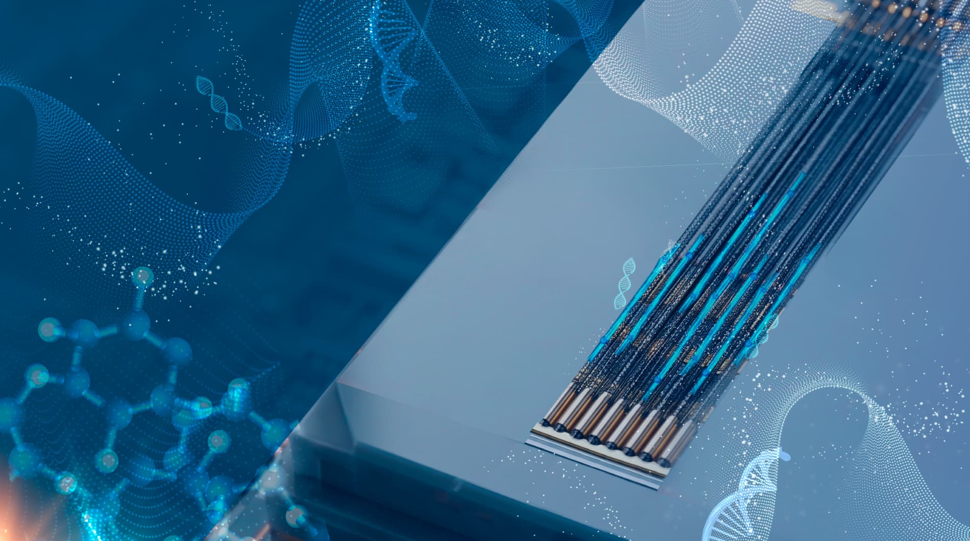
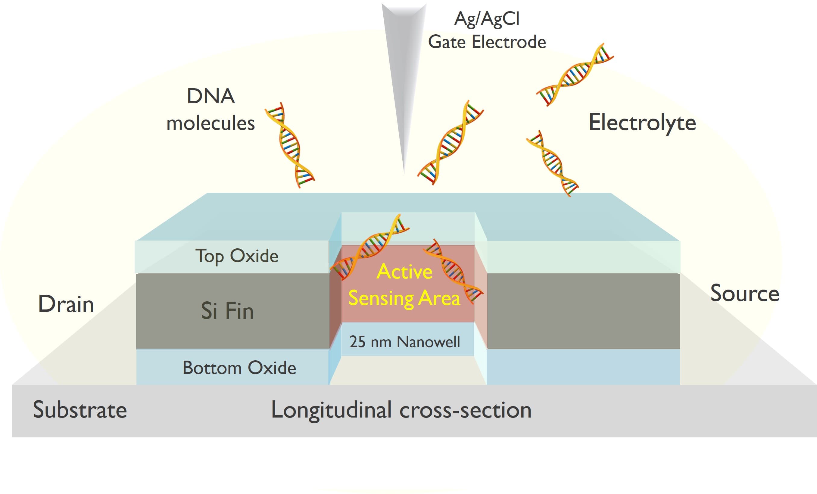
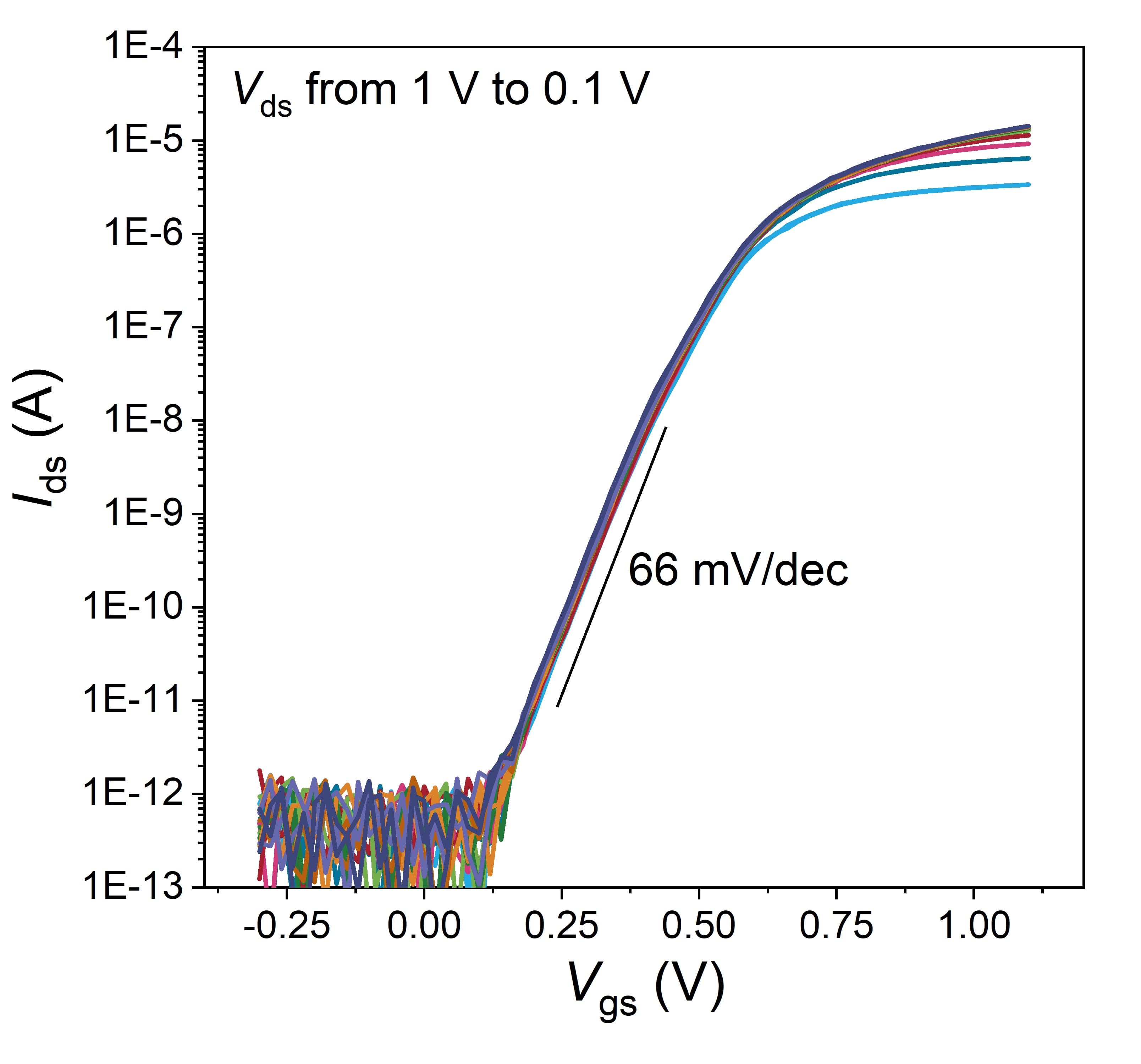
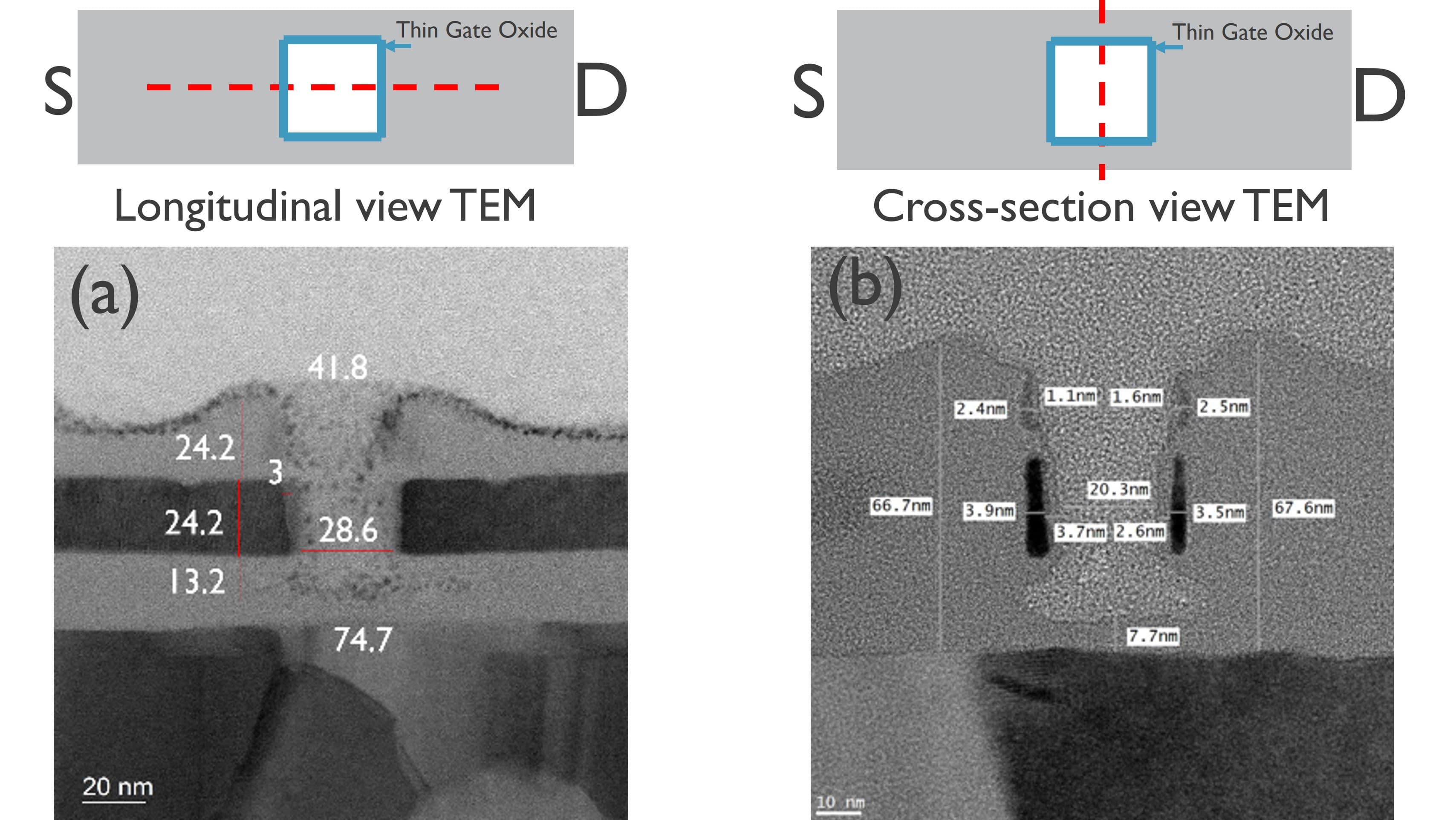
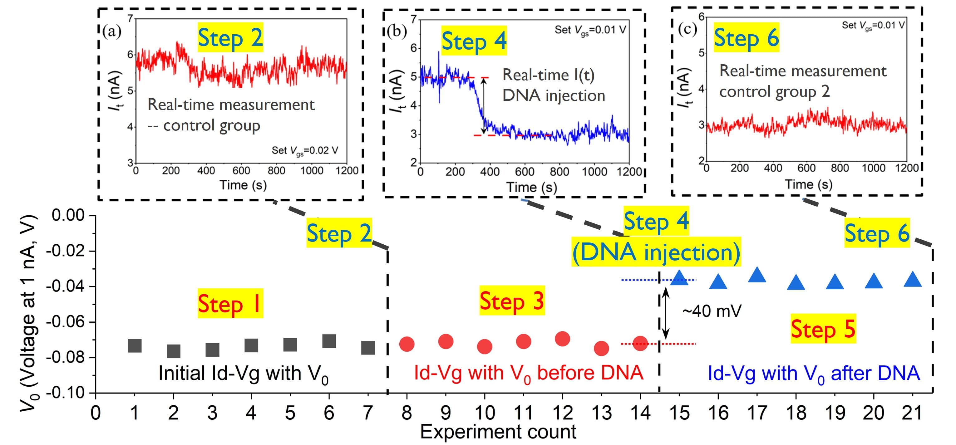
At the 2023 IEDM conference, imec unveiled another pioneering design – the nanowell FET. Building upon traditional FinFET principles, this innovation introduces an additional well in the nanowire that further enhances the sensitivity of the device. The device features a 35-40nm wide silicon FinFET with a 25nm nanowell as the active sensing area. Within the well, binding of an estimated ten short single-stranded DNA molecules boasts a clear signal of 40mV, which is double the signal achieved from the previous FinFET device. Noteworthy are also its near-ideal electrical properties, marked by a subthreshold swing of 66 mV/dec, close to the theoretical minimum of 60. This demonstrates that electrolyte gating effectively happened inside the nanowell.
The challenges of creating such a nanowell FET lay in the need to remove material while preserving the integrity of the entire semiconductor device. Imec's innovative processing techniques, such as sacrificial layers to enable the formation of the self-aligned nanowell, and precise material selection, including a C3N3 self-assembled monolayer coating, contribute to the device's reproducibility, reliability, and pioneering design.
Challenges and future frontiers
Future steps involve experimental verification of single-molecule detection potential, for both the current nanowell and the earlier developed FinFET biosensor, and exploration beyond DNA sensing. Imec also aims to explore nanopore FETs, enabling DNA sequencing and proteomics. Combined, these innovations showcase the burgeoning potential of transistors in parallel biosensing at the nanoscale.
This article appeared earlier in Power Electronics News and was presented at the 2023 IEEE International Electron Devices Meeting (IEDM) December 9-13.
Authors

Lijun Liu

Sybren Santermans
dr. Sybren Santermans holds a Ph.D. in Materials Engineering from the University of Leuven (KU Leuven), Belgium (2021) and joined the Electrical Function and Test (EFT) group post-Ph.D. at imec. His current focus lies in the characterization, modelling, and simulation of FET-based, nanopore, and electrochemical sensors designed for life science applications.
During his Ph.D., Santermans focused on the modelling and characterization of silicon bioFET sensors for a prospective high-throughput single-molecule sensing platform, in collaboration with imec. He obtained a Master of Engineering Science degree in nanoscience, nanotechnology, and nanoengineering with a focus on nanobiotechnology in 2017 at the University of Leuven.

Koen Martens
dr. Koen Martens, currently a principal scientist at imec, holds a Ph.D. in Electrical Engineering from the University of Leuven (KU Leuven), Belgium (2009). Since 2016, his research interests have centered around harnessing CMOS technology for life sciences applications, particularly in the realm of massively parallel biosensing for genomics and proteomics.
During his FWO postdoc, he conducted exploratory nanoelectronics research on the metal-insulator transition material VO2 with imec and IBM. He also played an active role in projects involving 2D materials and the STT MRAM Program at imec and worked on the voltage control of magnetic anisotropy (VCMA) with imec and Osaka University. Furthermore, he has contributed extensively to germanium and III–V MOSFET technology at both imec and Stanford University.