Imec demonstrates first wafer-scale fabrication of solid-state nanopores using EUV lithography
Breakthrough enables scalable, high-precision biosensing applications in life sciences and healthcare
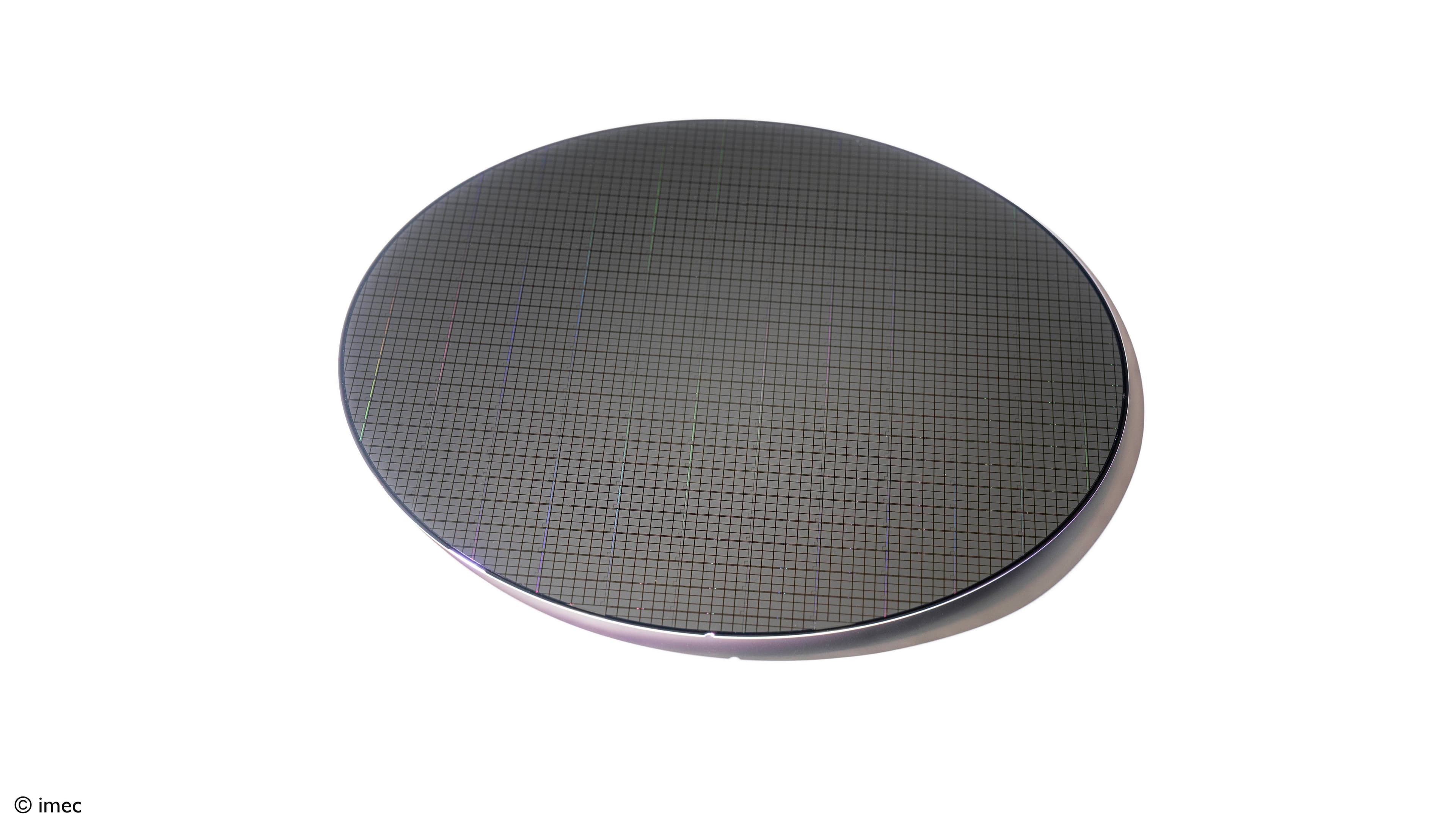
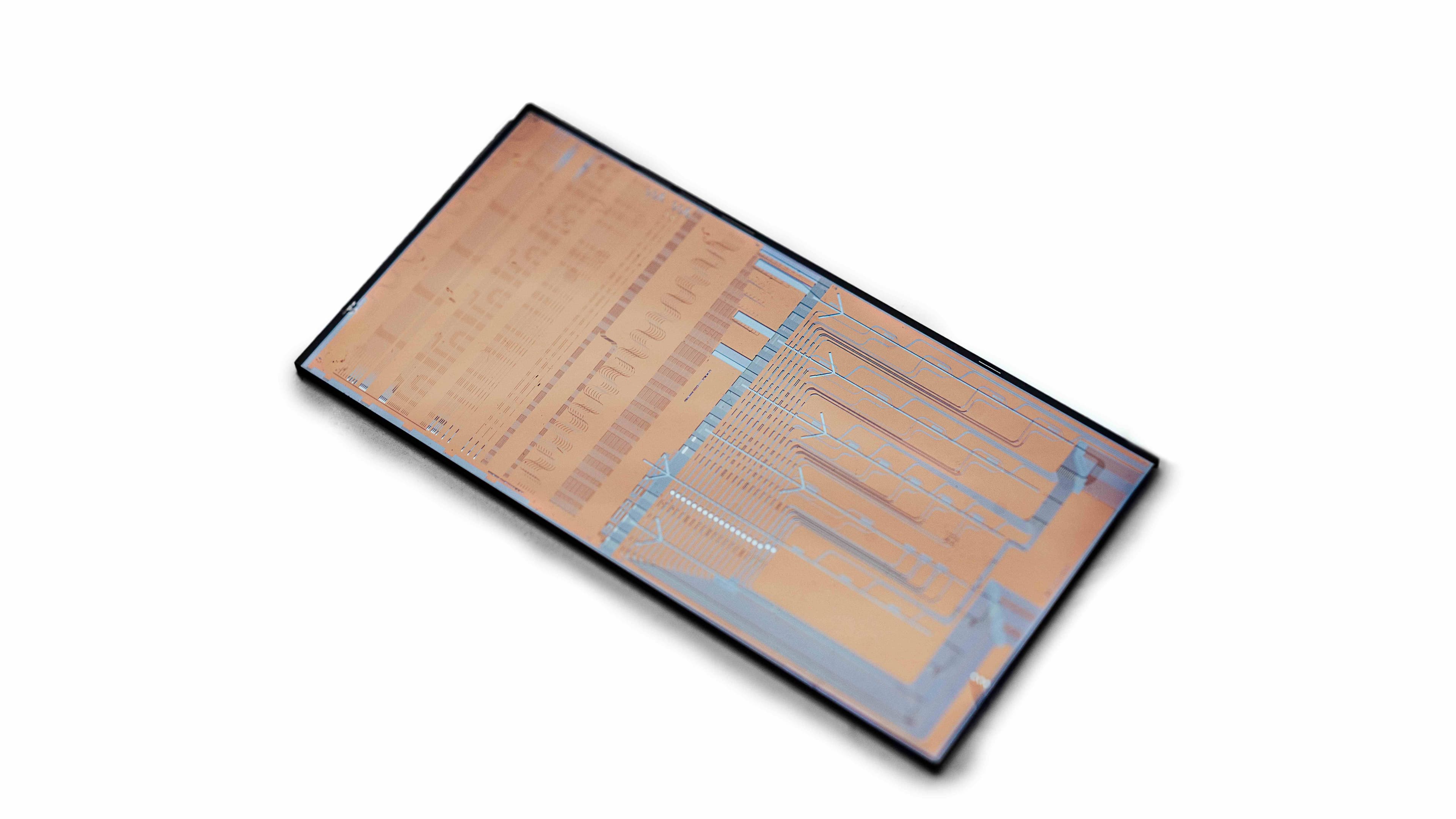
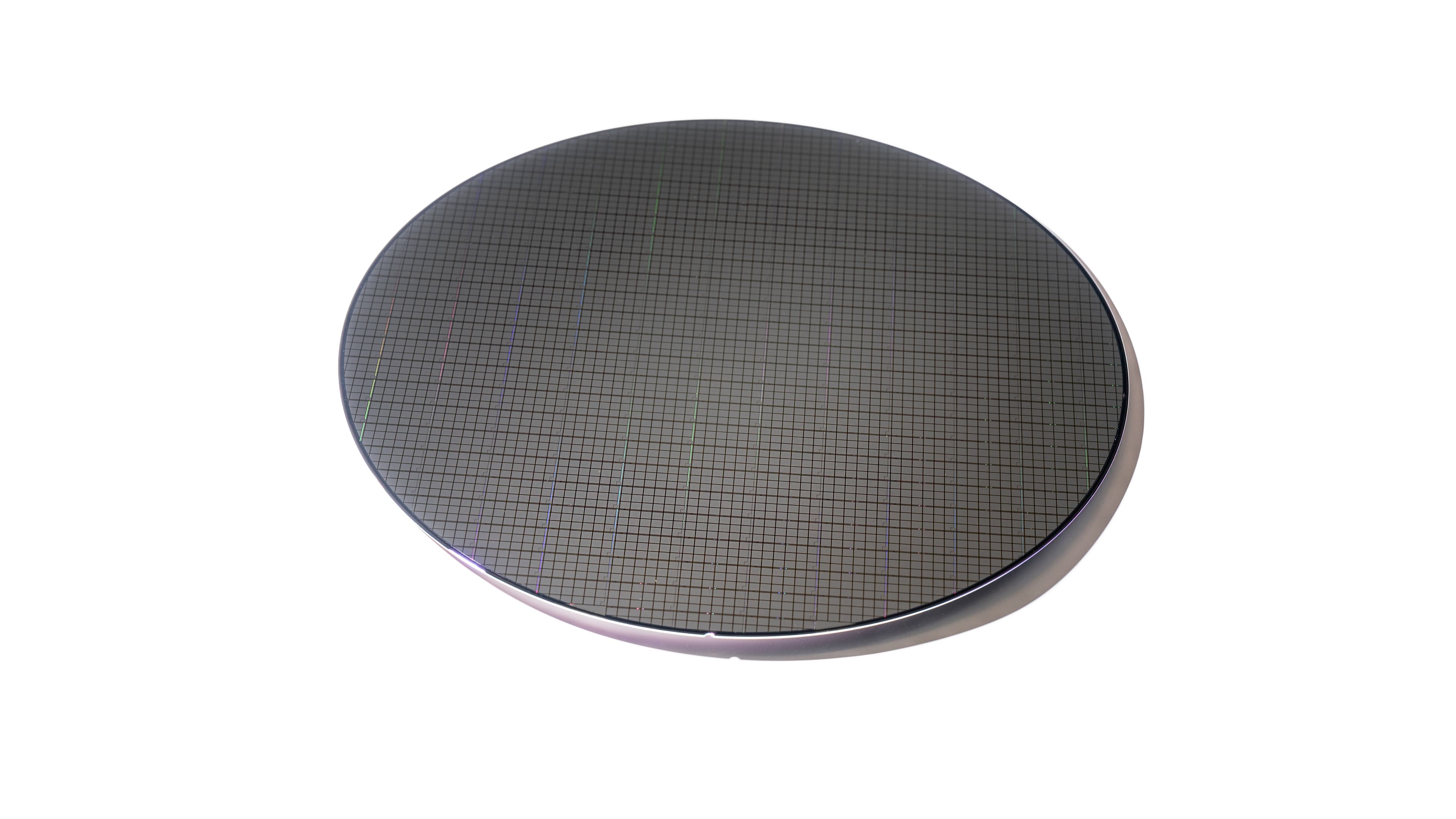
LEUVEN (Belgium), DECEMBER 9, 2025— At this year’s IEEE International Electron Devices Meeting (IEDM 2025), imec, a world-leading research and innovation hub in advanced semiconductor technologies, presents the first successful wafer-scale fabrication of solid-state nanopores using extreme ultraviolet (EUV) lithography. Solid-state nanopores are emerging as powerful tools for molecular sensing but haven't been commercialized yet. This proof of concept is a crucial step towards their cost-effective (mass) production.
Click here for regular updates on imec’s semiconductor research
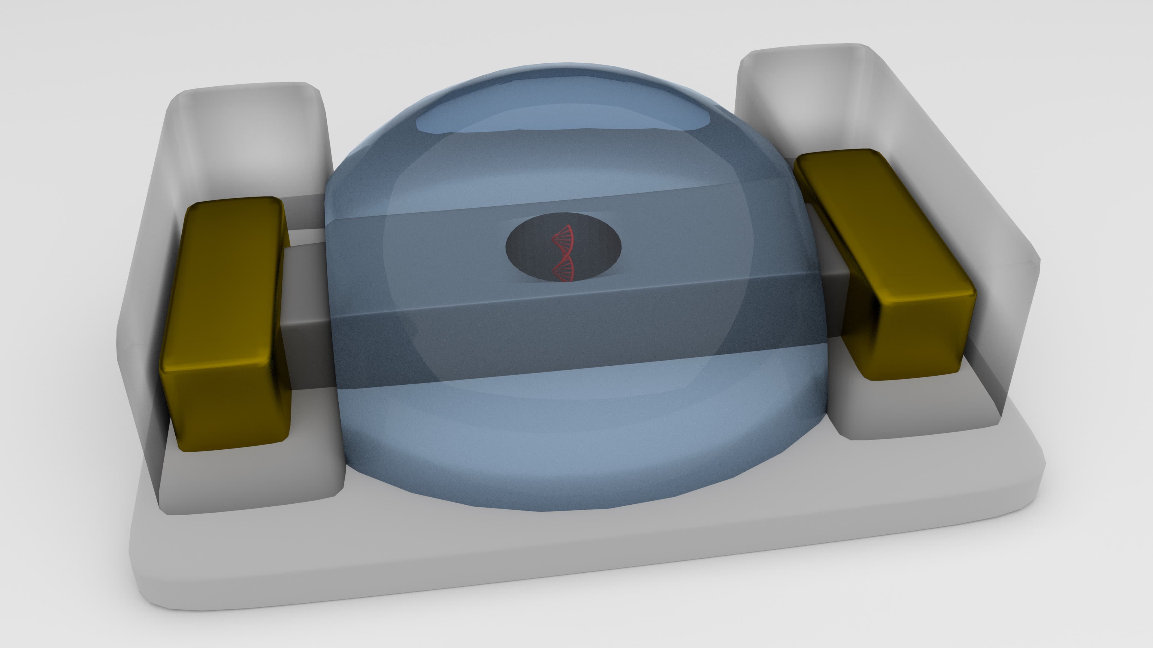
Nanopores are tiny holes - just a few nanometers wide - etched into silicon nitride membranes. When immersed in fluid and connected to electrodes, they allow individual molecules to pass through, generating electrical signals that can be analyzed in real time. Because the pore size can be easily adjusted, they offer a wide range of applications, from virus identification to DNA and protein analysis. This label-free, single-molecule detection method is key to next-generation diagnostics, proteomics, genomics, and even molecular data storage applications.
Biological nanopores, on the other hand, formed by proteins in lipid membranes, have enabled commercial sequencing platforms, but they are limited by stability and integration challenges. Solid-state nanopores overcome these limitations with robustness, tunability, and compatibility with semiconductor manufacturing, making them ideal for scalable, high-throughput sensing. But achieving nanometer-level precision and uniformity in solid-state pores across large areas remains a challenge. Current fabrication techniques are often slow and limited to the lab, delaying their widespread use for sensing applications.
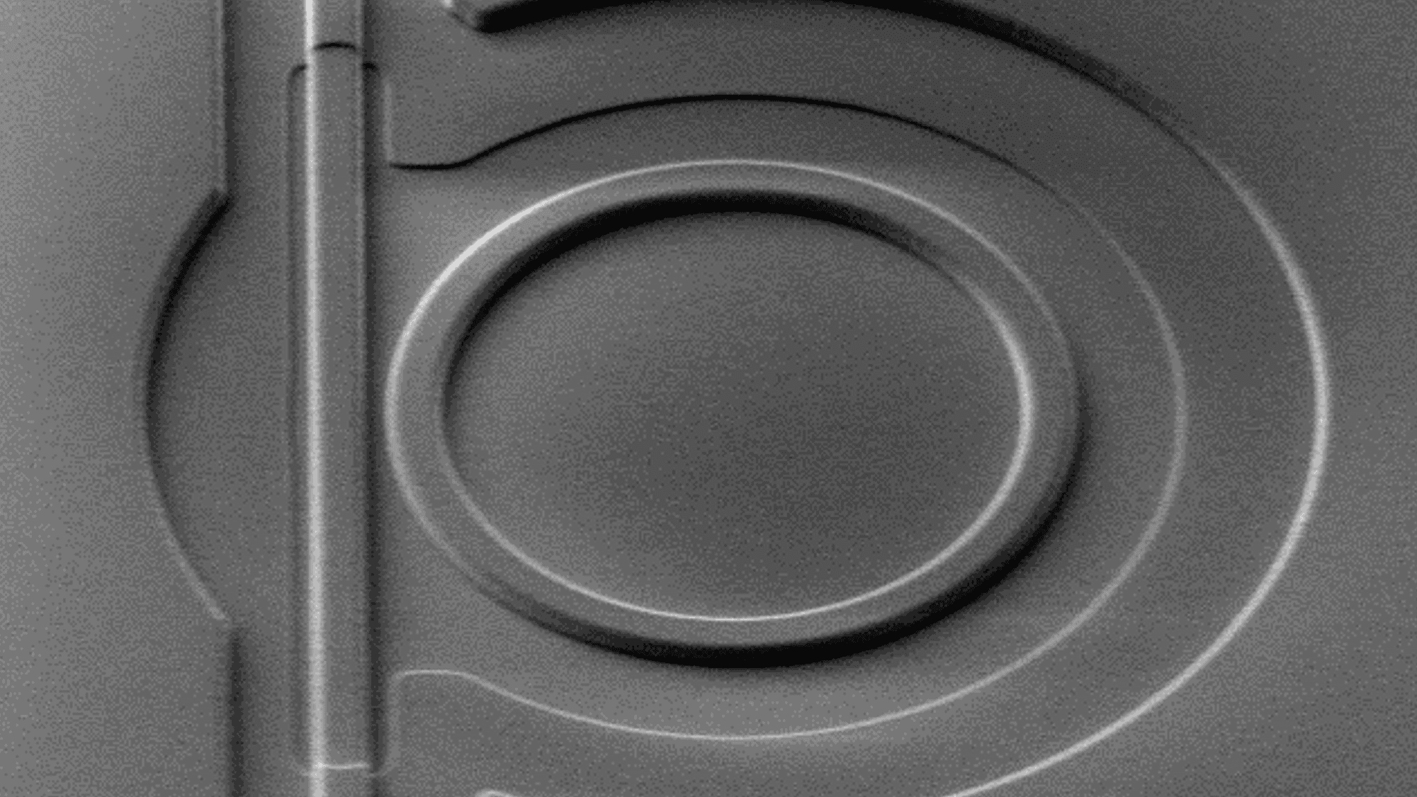
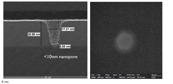
In a new paper presented at IEDM 2025, imec reports successful fabrication of highly uniform nanopores with diameters down to ~10nm across full 300mm wafers. The team combined EUV lithography with a spacer-based etch technique to achieve nanometer-level precision and reproducibility - two long-standing challenges in nanopore technology.
The nanopores were embedded in silicon nitride membranes and electrically characterized in aqueous environments. Translocation experiments with DNA fragments also confirmed high signal-to-noise ratios and excellent wetting behavior, validating the nanopores’ sensing performance with biological material.
“Imec is uniquely positioned to make this leap. We can apply EUV lithography – traditionally reserved for memory and logic – to life sciences. By leveraging our lithography infrastructure, we’ve shown that solid-state nanopores can be fabricated at scale with the precision needed for molecular sensing,” said Ashesh Ray Chaudhuri, first author and R&D project manager at imec. “This opens the door to high-throughput biosensor arrays for healthcare and beyond.”
Looking ahead, this feat can enable rapid diagnostics, personalized medicine, and molecular fingerprinting. Building upon the EUV nanopore advancements, imec is currently developing a modular readout system with scalable fluidics as a platform for application-relevant chemistry development. The team invites life science tool developers to use this platform to test their concepts and requirements.
At the 2026 IEEE International Solid-State Circuits Conference (ISSCC), the paper “A 256-Channel Event-Driven Readout for Solid-State Nanopore Single-Molecule Sensing with 193 pArms Noise in a 1 MHz Bandwidth” will be presented, showcasing a proof-of-concept ASIC readout developed by imec, to support next-generation custom nanopores.
About imec
Imec is a world-leading research and innovation hub in advanced semiconductor technologies. Leveraging its state-of-the-art R&D infrastructure and the expertise of over 6,500 employees, imec drives innovation in semiconductor and system scaling, artificial intelligence, silicon photonics, connectivity, and sensing.
Imec’s advanced research powers breakthroughs across a wide range of industries, including computing, health, automotive, energy, infotainment, industry, agrifood, and security. Through IC-Link, imec guides companies through every step of the chip journey - from initial concept to full-scale manufacturing - delivering customized solutions tailored to meet the most advanced design and production needs.
Imec collaborates with global leaders across the semiconductor value chain, as well as with technology companies, start-ups, academia, and research institutions in Flanders and worldwide. Headquartered in Leuven, Belgium, imec has research facilities in Belgium, across Europe and the USA, and with representation on three continents. In 2024, imec reported revenues of €1.034 billion.
For more information, visit www.imec-int.com
The imec group holds a global trademark portfolio, including word marks and combined figurative registered and unregistered trademarks, across national, regional, and international territories. Its lawful use requires prior written consent of IMEC in compliance with the IMEC branding guidelines, which may be updated periodically. The latest version is available upon written request.