Large-area optical sensors
Turn to imec for the development of new photodetectors, design of readout backplanes and integration of the two to enable large-area sensing applications.
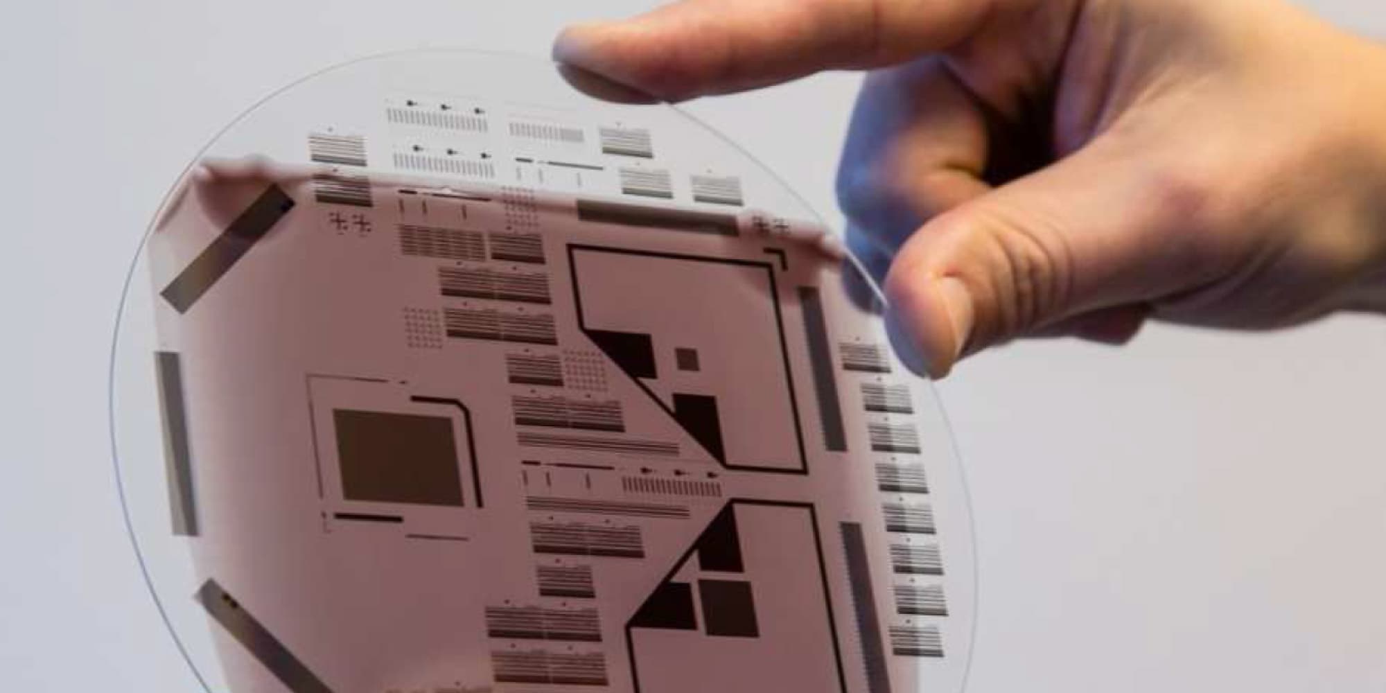
Arrays of photosensitive pixels distributed over large areas are crucial for important applications such as:
- x-ray detectors (radiology, mammography)
- fingerprint scanners (biometrics)
- curved imagers (inspection)
Such arrays are constituted of two components:
- The thin-film photodetector (TFPD) frontplane ensures the selection of the most appropriate sensor, with organic, quantum dot and perovskite absorbers to choose from.
- The thin-film transistor (TFT) backplane enables large sensing areas, flexibility and even transparency, with the manufacturing process compatible with flat-panel display (FPD) industry.
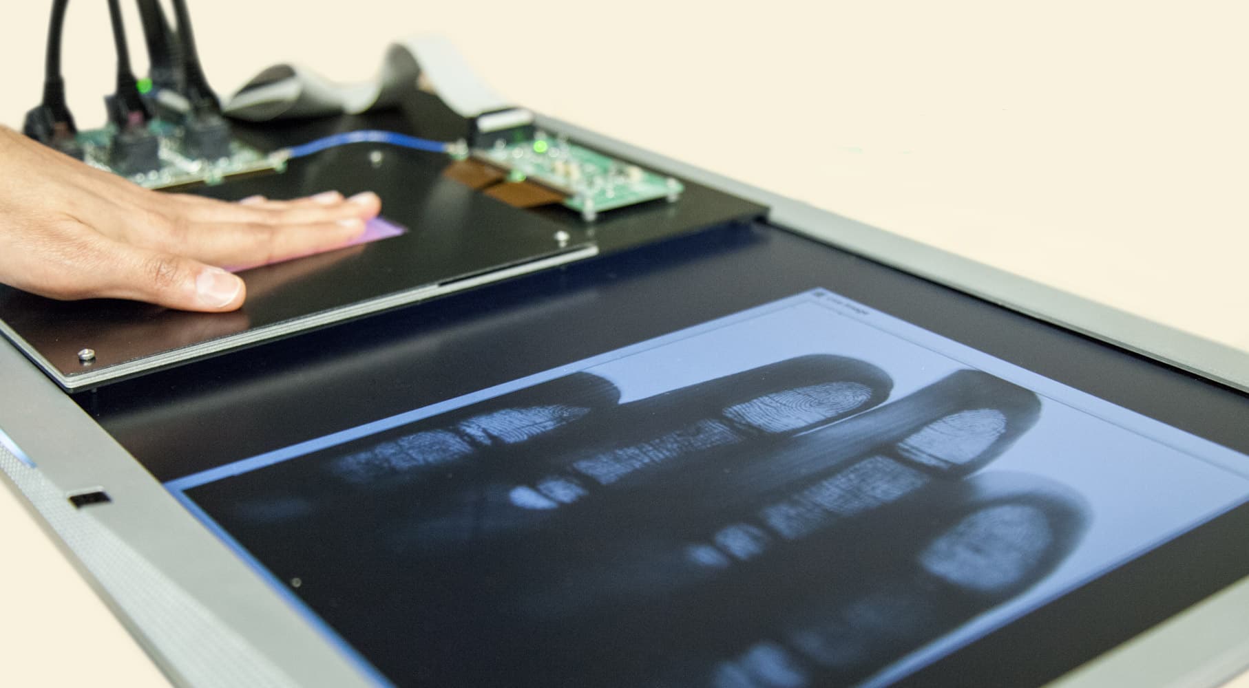
Imec specializes in the development of new photodetectors, design of readout backplanes and integration of the two.
Over the years, we have demonstrated proof-of-concept devices showing different modalities of large-area image sensors.
- Take a look at this video and this video about our award-winning fingerprint sensor concept.
- Read the press release about PYCSEL, a European-funded project to develop he world's first fingerprint sensor that combines printed pyroelectric PVDF-based layers above an IGZO-TFT active matrix on a flexible plastic foil.
- Visit the website of NEXIS, a Horizon 2020-project that looks into next-generation X-ray imaging systems
Imec not only helps you to address technological challenges. Thanks to our thorough knowledge of the industry, we function as your full-fledged strategic partner – right down to venturing support.
Click the button below to get in touch.
Links
Article in npk flexible electronics: Curved digital X-ray detectors
External linkImec unveils fully organic imager for X-ray applications
External linkImec and Holst Centre unveil fully-organic imager
External linkProject Site - DiCoMo: Direct conversion hybrid-organic X-ray detectors on metal oxide backplane
External linkSome examples of what imec has done
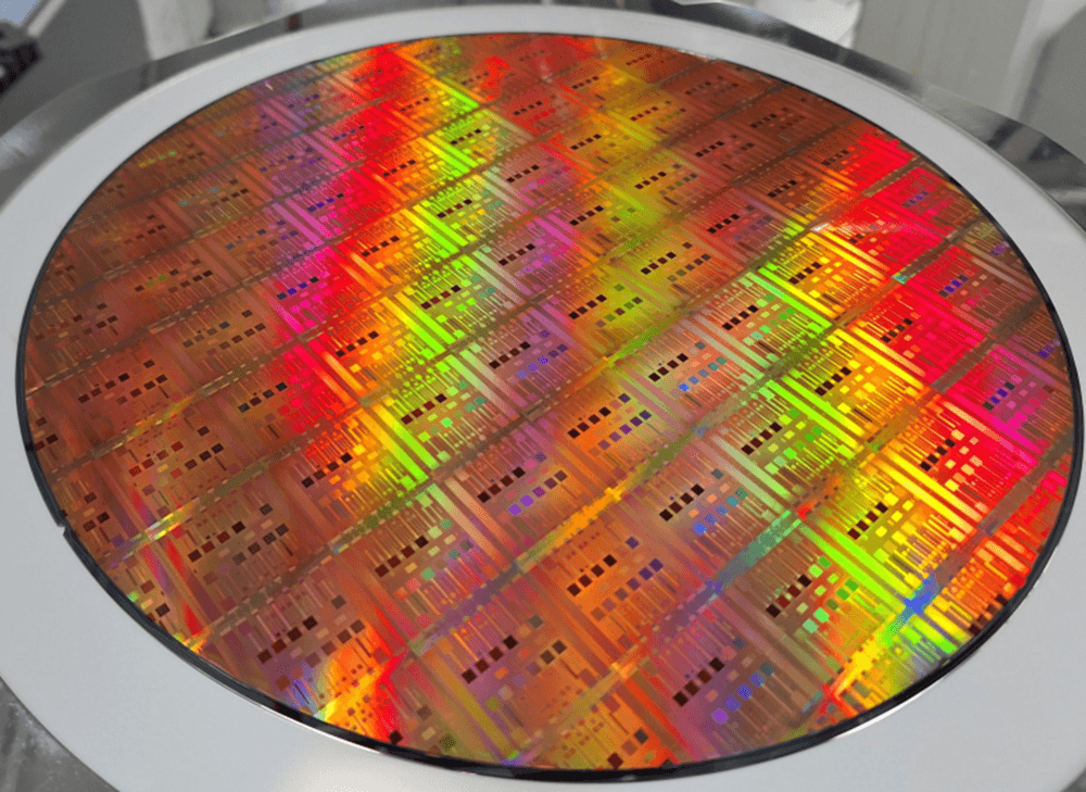
Imec successfully integrates colloidal quantum dot photodiodes (QDPDs) on metasurfaces developed on 300mm CMOS wafers
Pioneering approach makes compact, cost-effective, high-resolution multispectral shortwave infrared (SWIR) sensors accessible, enabling broad application in security, agriculture, automotive, aerospace, and more.
Read more
White paper: monolithic microsystems
Learn how to elevate your application to new heights with advanced functionalities on top of CMOS.
Read more
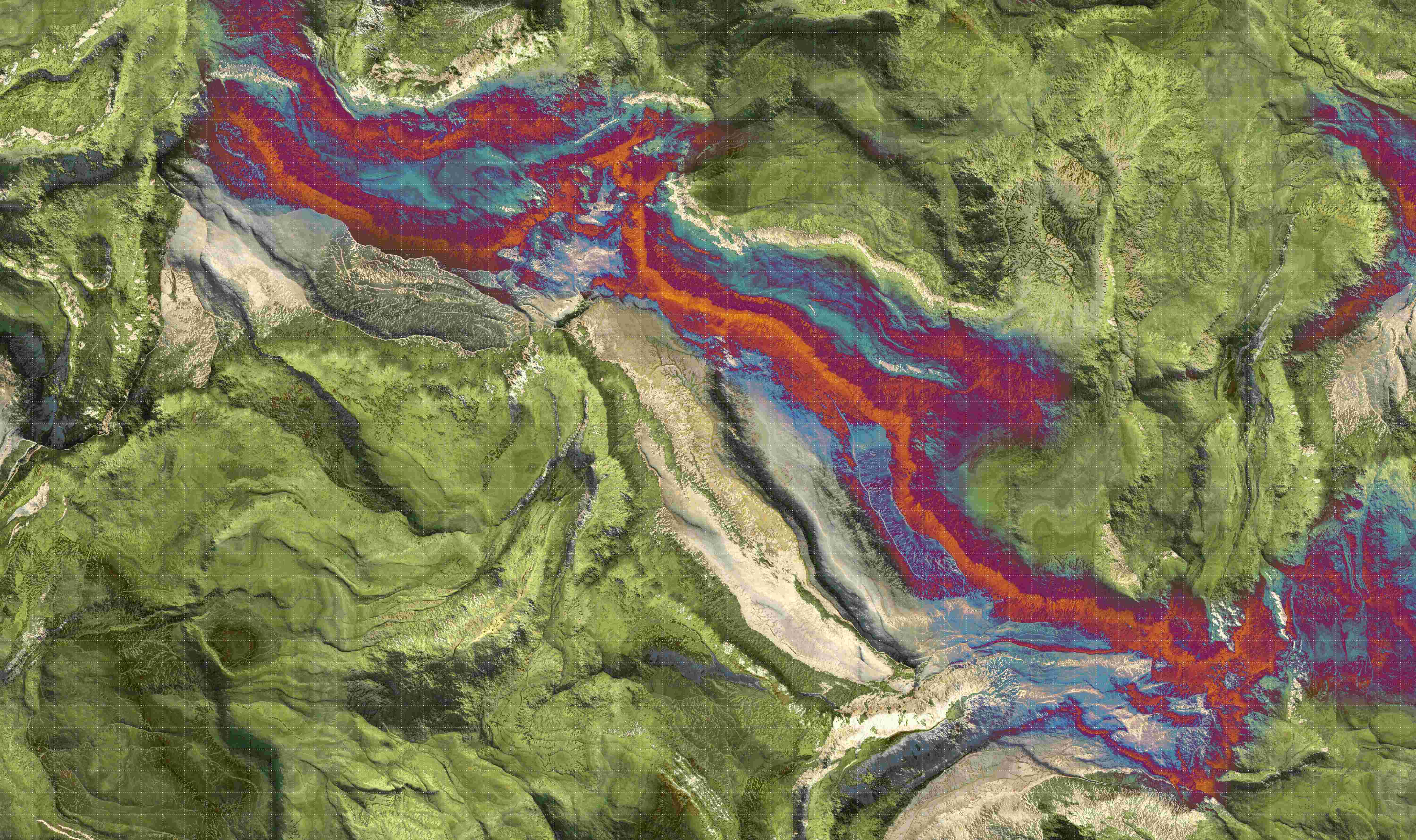
Imec hyperspectral sensor aboard newly launched earth-observation satellite
The IPERLITE mission is designed to demonstrate next-generation hyperspectral imaging technology in space. At the core is a hyperspectral sensor developed by imec.
Read more