Microfluidics
A whole lab on one cm². That’s what microfluidics ultimately enables. Here’s an overview of imec’s activities in this field.

Microfluidics allows the precise control and manipulation of fluids on an exceedingly small scale. Combined with sensing and actuating capabilities, this results in compact devices that are also known as labs on chips, enabling researchers and physicians to perform a variety of lab functions on tiny amounts of fluid (such as droplets). Through applications ranging from DNA analyses and advanced diagnostics to precision therapies, these technologies are revolutionizing the healthcare industry.
Over the years, imec built up extensive expertise in the construction of silicon and polymer microfluidic components, and in their monolithic integration with silicon electronics, micro-optics, and photonics – a project that received funding from the PhotonDelta National Growth Fund program.
Our R&D toolbox also includes the surface chemistry that is indispensable for microfluidic applications. We are able to implement vapor phase surface functionalization through:
- uniform wafer-level gas phase surface characterization
- site-specific surface treatment in micro- and nanoarrays enabling single-molecule functionalization
- uniform gas phase surface functionalization in closed microchannels
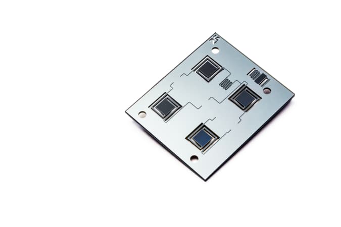

White paper: monolithic microsystems
Elevate your application with advanced functionalities on top of CMOS.
Silicon microfluidics
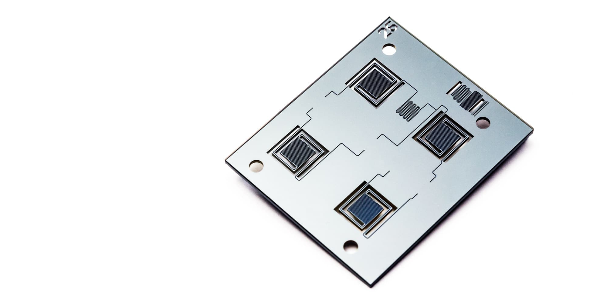
Which material should you choose for your microfluidic structures? Polymer is a good, cost-efficient option for less-demanding devices. But nothing beats silicon if your device needs extremely small features, integrates a variety of sensors or actuators within microfluidics, or requires massive integrated circuits. on a single chip.
Silicon fluidics are:
- reliable
- mass-producible
- suited for a wide variety of high-resolution and high-aspect-ratio structures
- readily combinable with a variety of silicon sensors, actuators and transistors
- high heat transfer rate allowing for ultra-fast heat transfer hence fluid thermal cycling
Imec uses photolithography to make silicon fluidic structures such as microchannels, -pillars and -reactors, mixers, droplet generators, capillary pumps and valves, mergers and splitters. We achieve diameters as small as 0.5 µm – 10 nm for devices such as nanopores.
Our silicon fluidics technology is key to groundbreaking applications such as:
- ultra-fast PCR microreactors that enable 40 cycles in 3 minutes
- programmable droplet processors
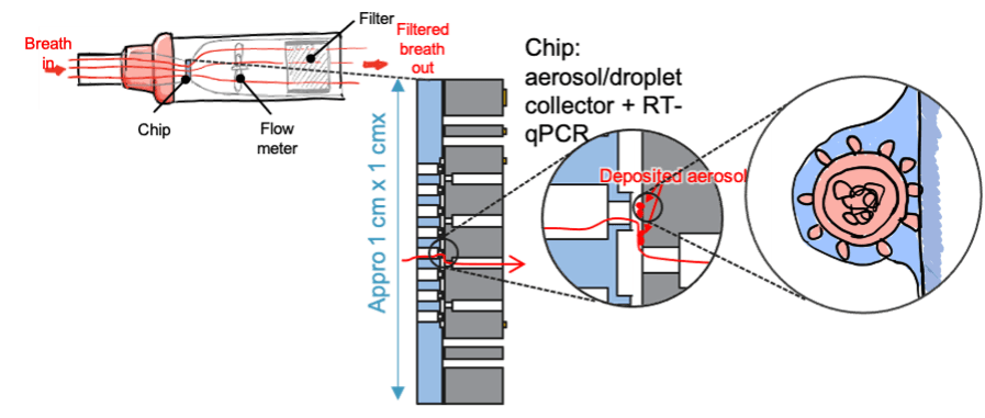
- aerosol capture, using a large array of tiny nozzles – for instance for breath analysis
- crossflow filters for on-chip enrichment and plasma separation
- autonomous capillary fluidics devices for point-of-care diagnostics, such as the products developed by imec’s spin-off miDiagnostics
Active microfluidics
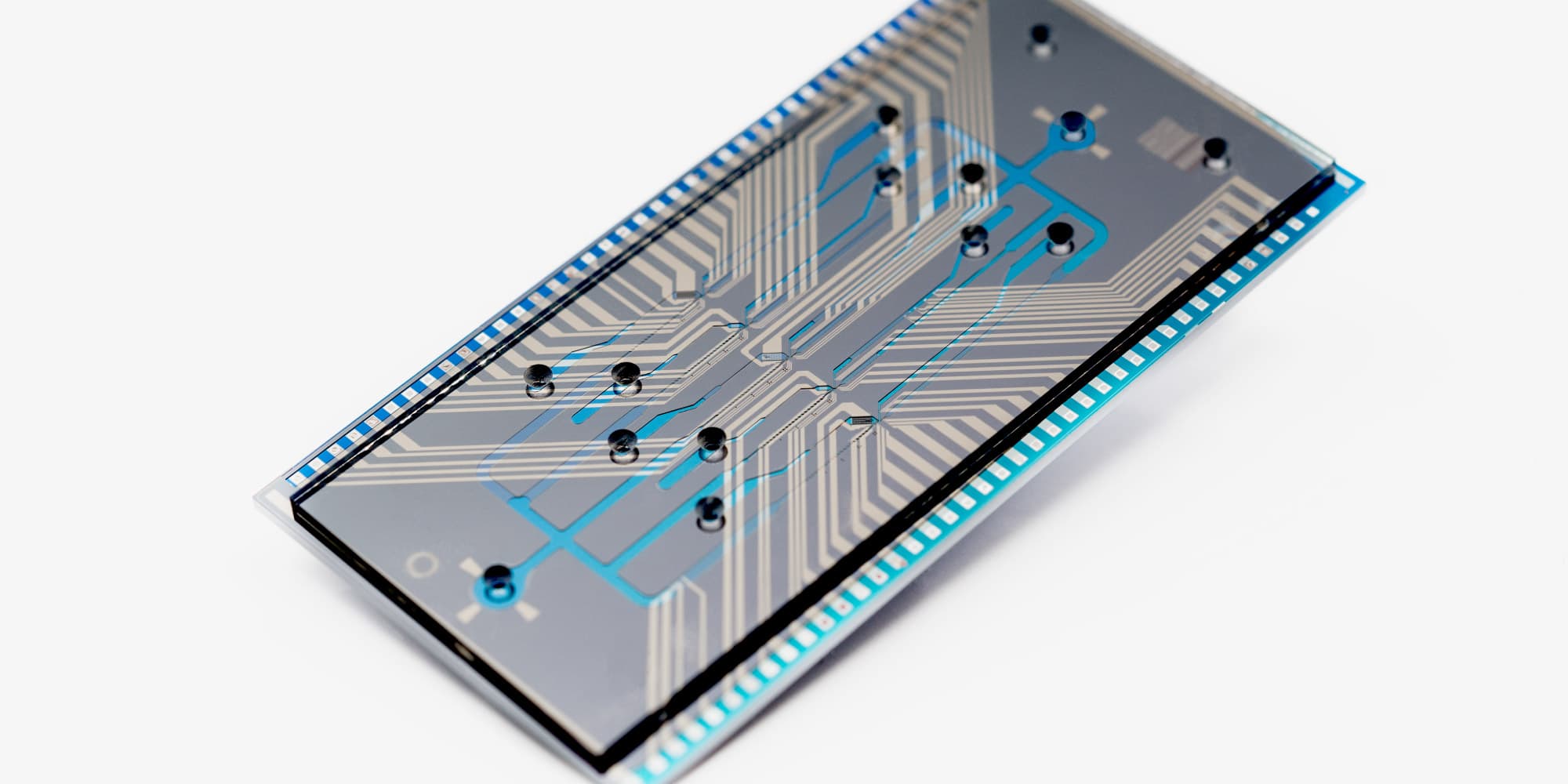
Active fluidics benefit from the integration of energized actuators with silicon fluidics. The active actuators are often electrical, acoustic or optical components fabricated in the microfluidics structures using the same set of tools in a semiconductor foundry.
Some examples of active fluidics devices are:
- fast vapor bubble arrays for high-speed jet-flow cell sorting
- dielectrophoretic cell and biomolecule manipulations
- fluidic actuation by AC electro-osmosis
Integrated fluidics system
The convenient integration of silicon fluidics with other components on a CMOS platform allows the creation of automated systems for complex fluid handling. One compact chip is then able to perform all the necessary functions without resorting to bulky I/O peripherals.
Integrated fluidic systems can take the form of:
- continuous fluidics – Miniaturized pumps and microvalves enable on-chip fluidic handling. Or capillary fluidics allow for complex networks without the need for pumps altogether.
- droplet fluidics – Droplet actuation, merging, sorting and splitting ensure complex fluidic actions in a true microreactor. Electrowetting-on-dielectric (EWOD) allows for a generic, programmable droplet processor with high-throughput potential and multi-core parallel processing.
Microfluidics packaging
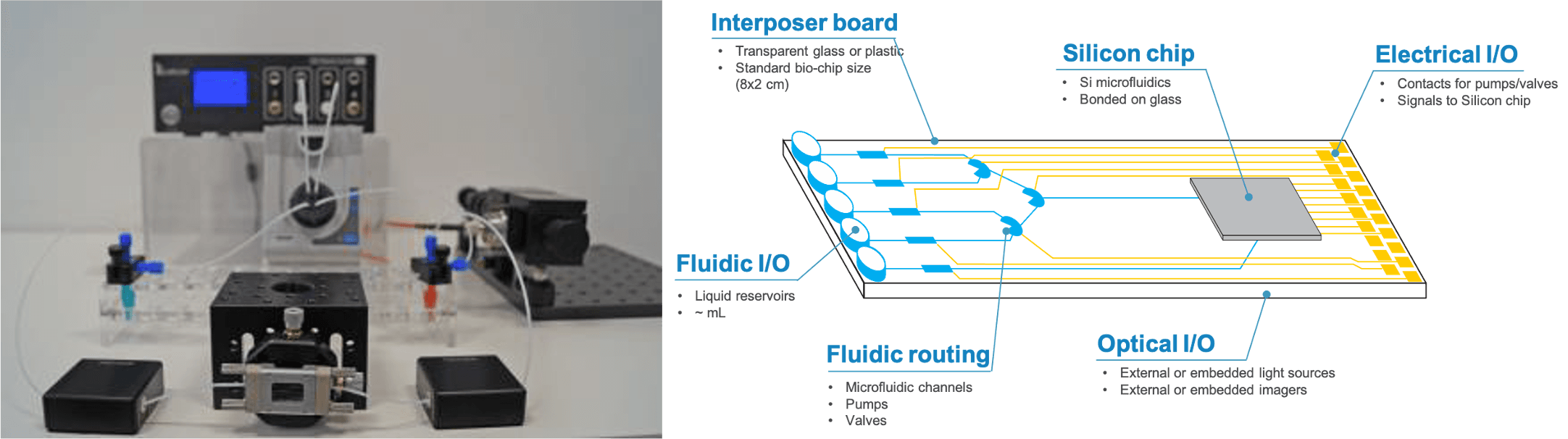
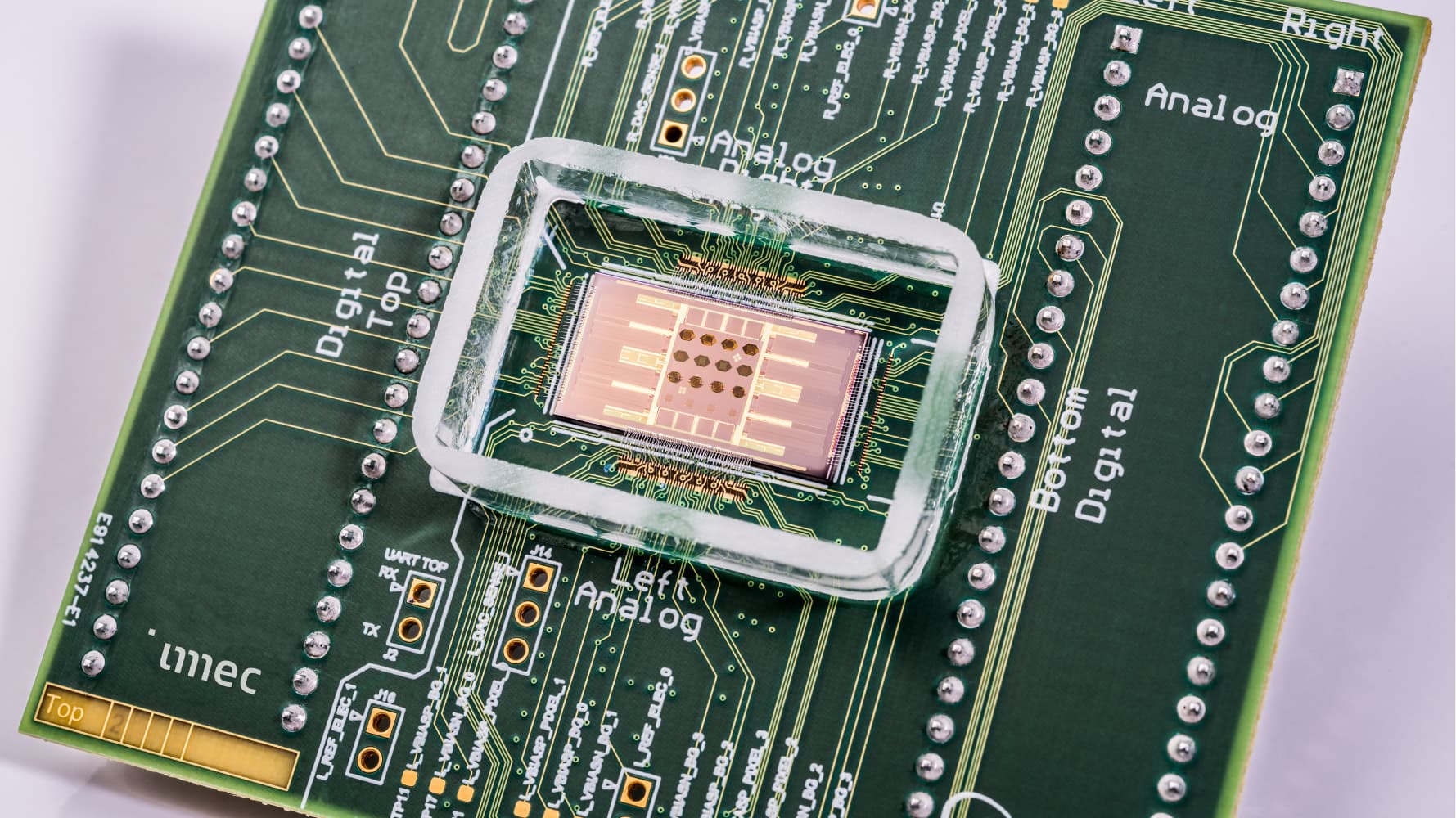
With the move towards integrated fluidics comes a need for more advanced packaging solutions that combine silicon chips with microfluidics.
Imec is working together with industrial partners on the microfluidics chip packaging workflows using commercial components and solutions such as adhesives, partial dicing, and pick-and-place. This is ideal for simple fluidic input/output requirements due to the low cost and high industrial readiness.
For rather complex packaging needs, such as massively parallel electrical, optical and fluidics interfacing, we’re also adapting fan-out wafer-level packaging (FOWLP) capabilities for their application to microfluidics. This would provide:
- increased mass-manufacturability
- advanced multi-connectivity
- true miniaturization
- potential to package multiple CMOS ICs on one carrier
Work with us
Want to leverage our expertise and infrastructure to develop your microfluidic or integrated fluidic device? We support you from concept to product, including:
- microfluidic simulations
- design and prototyping
- functional testing
- low-volume production
Imec not only helps you to address technological challenges. Thanks to our thorough knowledge of the health and pharma sector, we function as your full-fledged strategic partner – right down to venturing support.
Click the button below to get in touch.
Scientific publications
De Moor et al. “Electric field gradient focusing with electro-osmotic flow to reduce analyte dispersion: Concept and numerical investigation”, Journal of Chromatography A, (2023)
External linkStakenborg et al. “Molecular detection of SARS-COV-2 in exhaled breath at the point-of-need”, Biosensors and Bioelectronics, (2022)
External linkQing, et al. “Ultra-fast, sensitive and quantitative on-chip detection of group B streptococci in clinical samples”, Talanta, (2019)
External linkSeungkyu et al. “CMOS-compatible selective biofunctionalization using a patterned sacrificial layer approach”, 12th International Workshop on Engineering of Functional Interfaces, (2019)
External linkDe Wijs et al. “Micro vapor bubble jet flow for safe and high-rate fluorescence-activated cell sorting”, Lab on a chip, (2017)
External linkHuang et al. “Dielectrophoretic discrimination of cancer cells on a microchip”, Applied Physics Letters, (2014)
External linkMajeed et al. “Silicon Based System for Single-Nucleotide-Polymorphism Detection: Chip Fabrication and Thermal Characterization of Polymerase Chain Reaction Microchamber”, Japanese Journal of Applied Physics, (2012)
External linkOther technology platforms
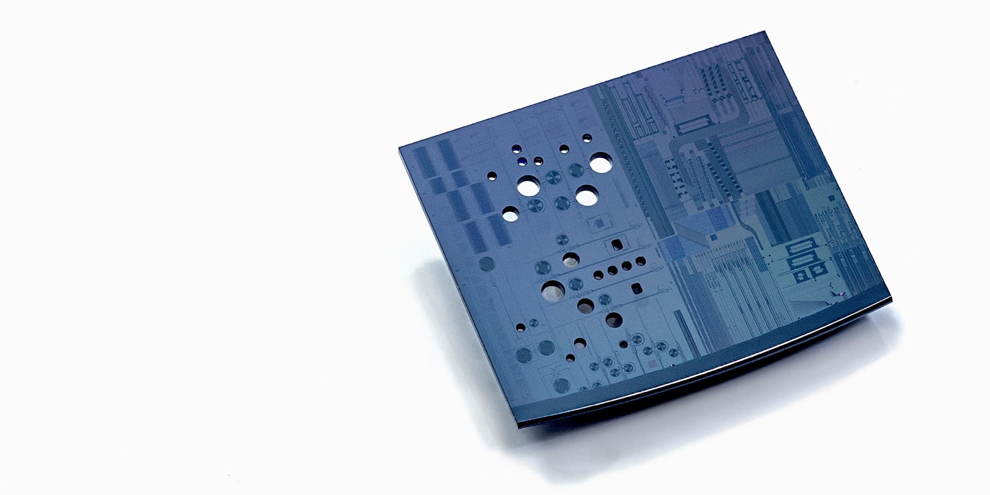
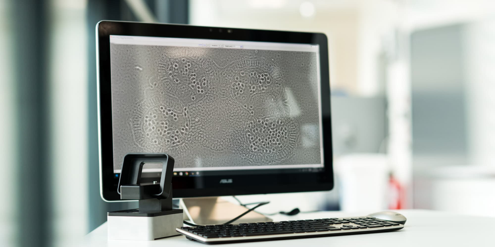
High-throughput cytometry and cell sorting (FACS)
Sort up to 30 million cells per minute on one cm2

Read more
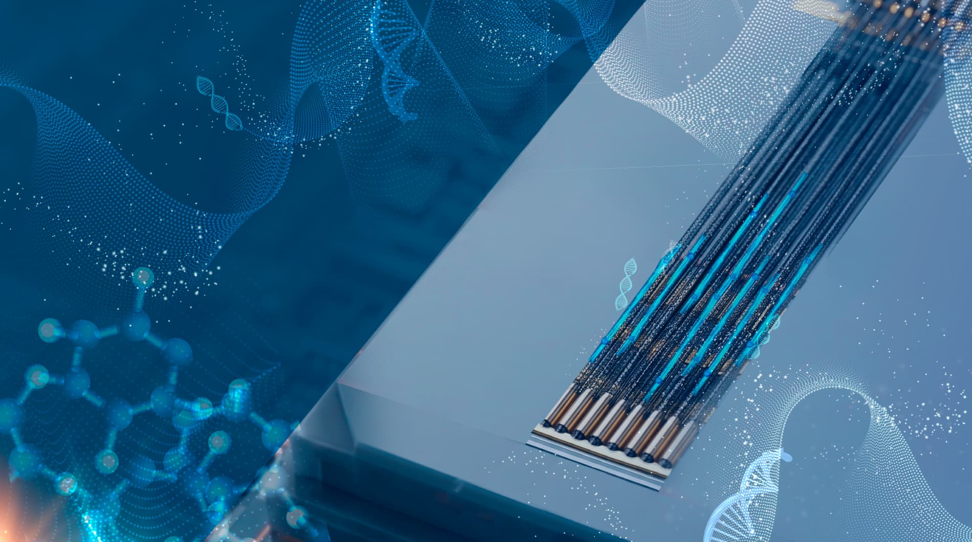
Towards scalable single-molecule biosensing using carbon nanotube FETs
Imec achieves real-time biomolecule detection using a wafer-scale bioFET approach, marking a promising step towards high-throughput sensing for genomics and proteomics.
Read more
Programmable droplet processor
Imec’s programmable droplet processor allows steering millions of droplets at pixel level, enabling fully automated enrichment, purification, and separation workflows through programmable droplet interactions.
Read more
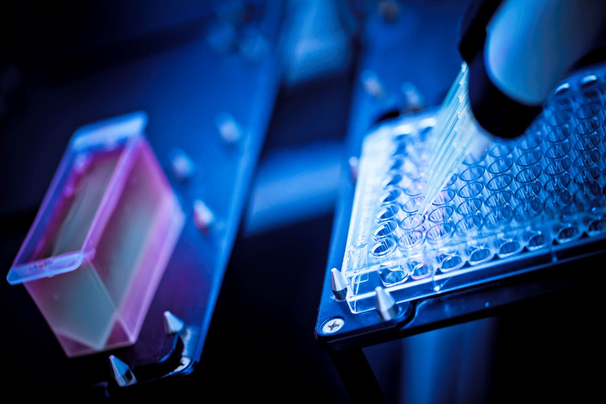
Imec builds nanopore platform for real-world assay innovations
Imec has made significant progress on its solid-state nanopore system that will enable life science companies to test and develop assays for single-molecule sensing. It is a cost-effective (mass-manufacturable), high-throughput solution.
Read more