Ultrasound transducer technology platforms
Take advantage of imec’s MEMS-based ultrasound transducer expertise and foundry-installed platform to develop your innovative ultrasonic solutions.
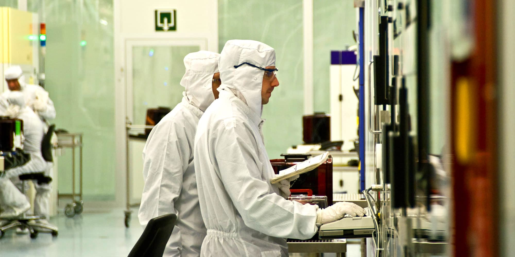
Ultrasound transducers are structures that convert electrical signals into ultrasonic waves – and vice versa.
Conventionally, ultrasound transducers are made in piezo-ceramic materials, are bulky and cannot be easily put in arrays as the wiring would be massive.
In contrast to these conventional devices, MEMS-based ultrasound transducers enable:
- more compact form factors
- a wider range of frequencies
- closer integration with a CMOS driver
- mass-producibility in standard silicon foundries
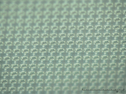
Imec has years of experience and a solid track record in developing CMOS-compatible Piezoelectric Micromachined Ultrasound Transducers (PMUT), and developed a foundry-installed platform for this technology.
Ultrasound transducer applications
We all know ultrasound technology from applications that have been around for decades, such as prenatal imaging. But MUTs, and their close integration with integrated circuits, allow for the development of more complex use cases.
Some of these applications rely on MUT technology to enable more subtle forms of sensing, such as fingerprint scanning, gesture recognition, or neuromodulation/brain stimulation.
Other applications extend the usefulness of ultrasound from sensing to actuation:
- directed sound
- wireless power delivery
- remote control of devices, such as smartwatches
- VR/AR
- remote surgery
- imaging (e.g. echography)
- ...
Are you looking to develop such innovative ultrasonic applications? Then imec is ready to support you, from technology selection, requirement analysis, modeling-simulation, design and prototyping to low- and even high-volume manufacturing.
Silicon-based ultrasound transducer technology platform
Do you want to turn your great idea into a manufacturable solution? Then it can be a challenge to find a foundry that’s willing to take up your project. Especially if your production volume – at least in its initial phase – is expected to remain low.
Thanks to its established collaboration with a foundry partner for PMUT technology, imec gives you access to elaborate in-foundry capabilities. Our ultrasonic actuators are directly processed on a silicon CMOS driver, resulting in a single-chip solution that is highly efficient and supports high-resolution applications.
Because innovative ultrasound applications often require a substantial deviation from standard frequencies, imec, together with its foundry partner tunes the PMUT technology platform to your needs. Thanks to our in-house infrastructure and expertise, we perform all the development steps quickly and efficiently. What remains is a short ramp-up to production at our trusted foundry partner.
Large-area ultrasound transducer technology
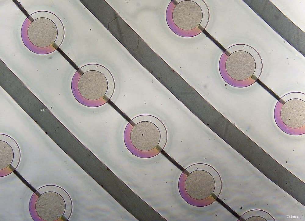
Are you intrigued by the possibility of integrating ultrasound transducers on larger surfaces (areas in the order of several tens to hundreds cm2)? Parallel with its CMOS-compatible PMUT technology, imec is working on a new display-manufacturing-compatible platform that’s suited for large-area electronics.
The first proofs of concept of this technology have emerged, as shown in the picture below.
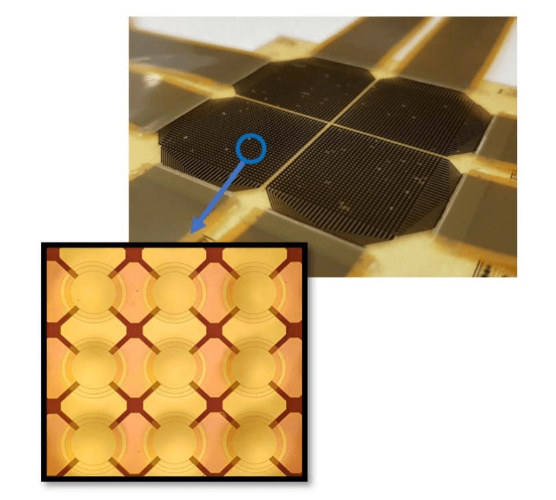
Imec ultimately aims at integrating these PMUT arrays with thin-film transistor backplanes (as the driving electronics) and fabricate them in unprecedented array sizes in display-manufacturing-compatible technology platforms.
Let us know if you want to know more about this exciting new research avenue.
Want access to our expertise and capabilities?
To realize ultrasound transducer devices towards your specifications, imec has design and modelling capabilities and has installed in-foundry PMUT processing capabilities.
We offer you:
- process/stack tuning tailored to the specifications of your application (frequency, power, sensitivity, size, radiation pattern, ...)
- design (electro-mechanical simulation, acoustic, device, sub-system, TFT and Si ASIC)
- characterization and demonstration (in-lab)
Imec not only helps you to address technological challenges. Thanks to our thorough knowledge of the imaging and sensing sector, we function as your full-fledged strategic partner – right down to venturing support.
Click the button below to get in touch.
Read more
A sneak peek at next-generation ultrasound imaging
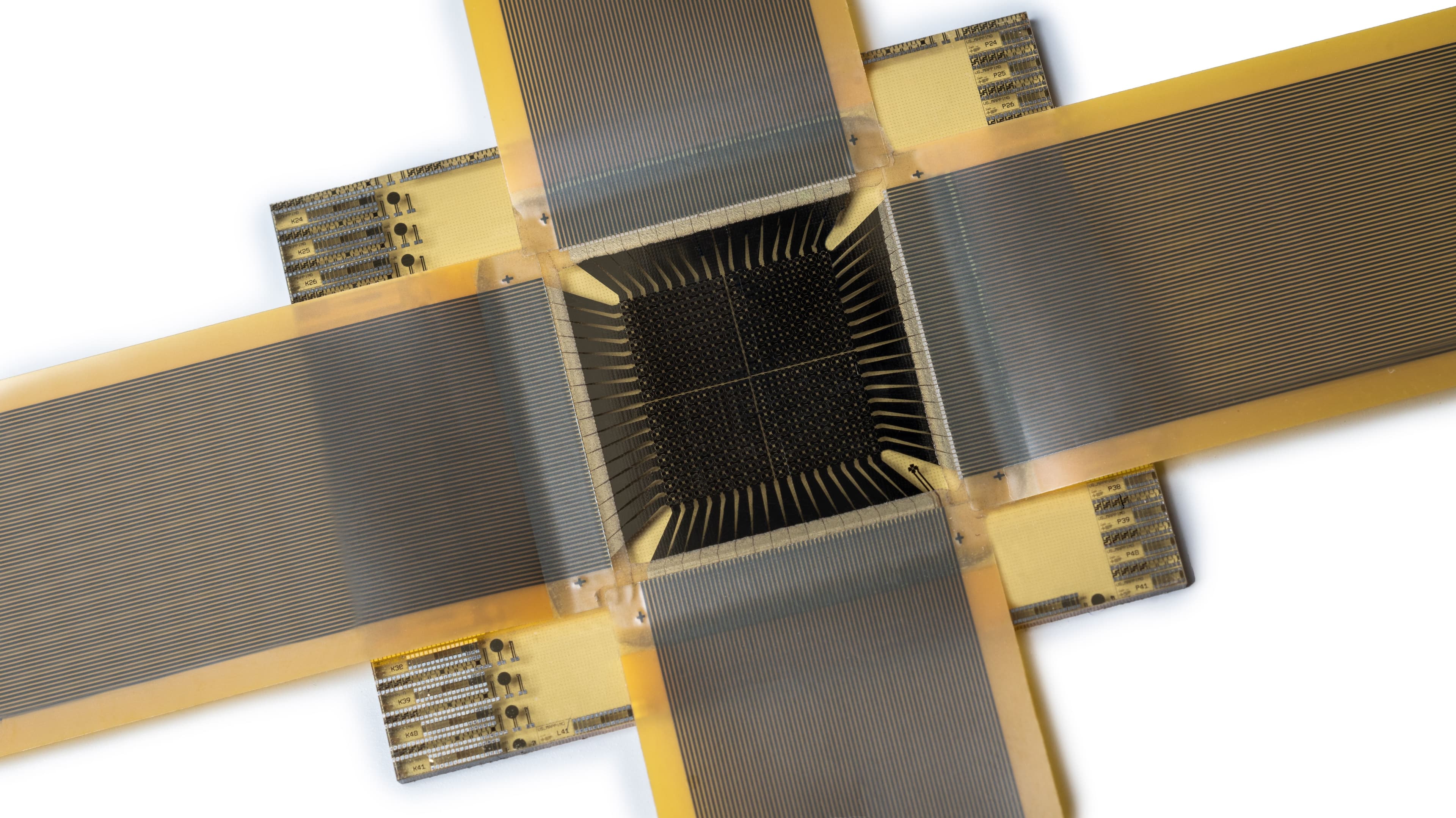
First demonstration of a flat-panel-display compatible ultrasound platform paves the way for large-area and curved surface applications.
Read more
Imec demonstrates flat-panel-display-compatible pMUT technology for emerging ultrasound applications
Read more
ITF USA 2026 at SEMICON® West
From silicon to systems: building the AI future The pace of AI evolution leaves little room for certainty. Yet, several trends are clear: AI agents increasingly collaborating in orchestrated ecosystems are on the rise. Physical AI is a crucial next step, including (humanoid) robots transforming our homes and workspaces. In parallel, AI – just like advances in quantum computing – could help unlock breakthroughs in fields such as physics and biology. Building the AI future starts with a solid hardware foundation – from high-performance, energy-efficient compute in the data centers to low-power, real-time inference at the edge. ITF USA at SEMICON® West presents the building blocks for shaping the AI future. On October 12 in San Francisco, we take stock of the full AI deep-tech stack: from silicon to systems, from research to manufacturing. Discover ITF USA
View event