Imec demonstrates semi-damascene interconnects with fully self-aligned vias at 18nm metal pitch
Two-metal-level semi-damascene module yields excellent line/via resistance and reliability – a world first

In short
Semi-damascene integration is an attractive, cost-effective approach to extend interconnect process flows below 20nm metal pitch.
This article presents the first experimental demonstration of a functional two-metal-level semi-damascene module at 18nm metal pitch, with fully self-aligned via.
The results were presented at VLSI 2022.
Introducing semi-damascene integration in the back-end-of-line roadmap
For more than 20 years, Cu dual-damascene has been the workhorse process flow for building reliable interconnects. But when dimensional scaling continues and metal pitches become as tight as 20nm and below, the back-end-of-line (BEOL) increasingly suffers from RC delay due to a dramatically growing resistance-capacitance (RC) product. This issue has forced the interconnect community to look for alternative integration schemes and metals with better figures of merit at tight metal pitches.
About five years ago, imec initially proposed semi-damascene as a viable alternative to Cu dual-damascene for integrating the most critical local (Mx) interconnect layers of the 1nm (and beyond) technology nodes.
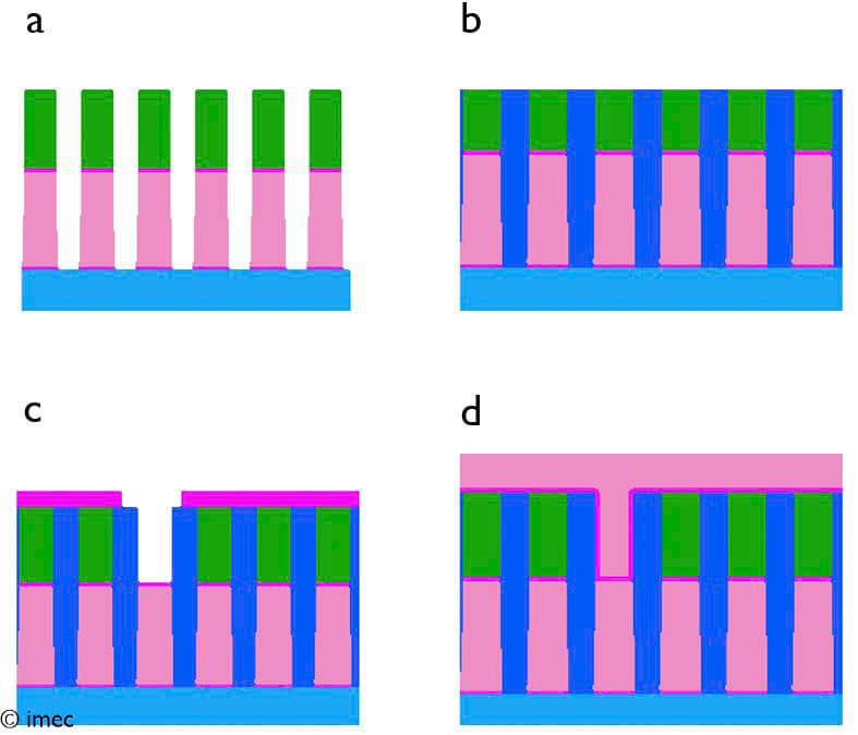
Unlike dual-damascene, semi-damascene integration relies on the direct patterning of the interconnect metal for making the lines (referred to as subtractive metallization), and chemical mechanical polishing (CMP) of the metal is not needed for completing the process flow. The vias that connect subsequent interconnect layers are patterned in a single-damascene fashion, then filled with metal and overfilled - meaning that the metal deposition continues until a layer of metal is formed over the dielectric. This metal layer is then masked and etched to form the second interconnect layer with an orthogonal line. After metal patterning, the gaps between the lines can be filled with a dielectric or used to form (partial) airgaps at the local layers. Note that in a semi-damascene flow, two layers (via and top metal) are formed in one go, just like for conventional dual-damascene. When benchmarked with dual-damascene, this makes it effectively cost-competitive (see figure 2).
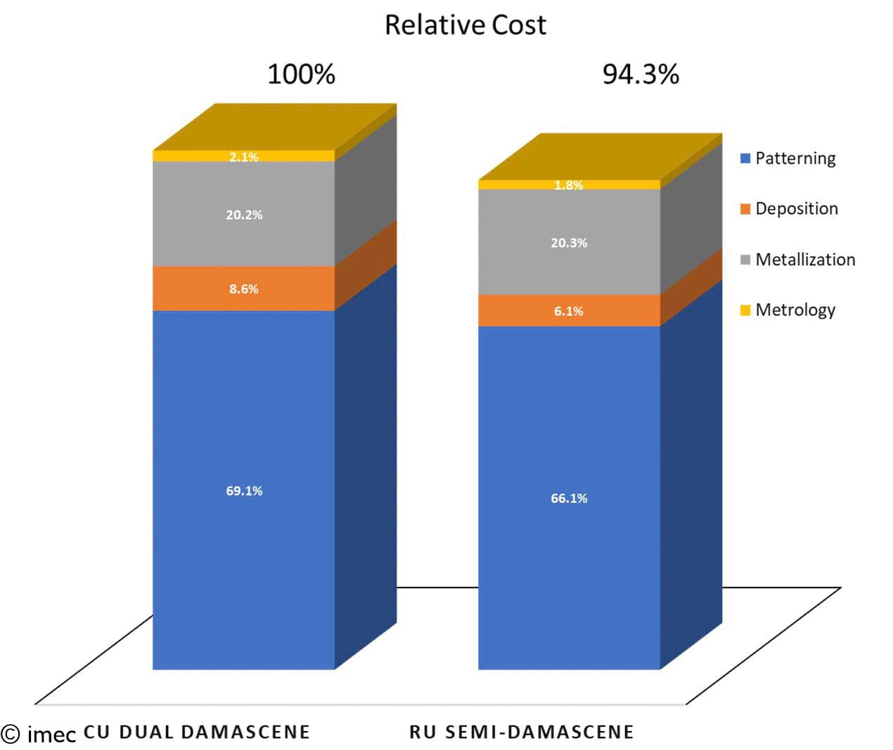
Benefits of a semi-damascene integration flow
Semi-damascene promises several advantages over Cu dual-damascene at tight metal pitches. Zsolt Tokei, imec fellow and program director of nano-interconnects at imec: “Firstly, it allows for higher line aspect ratios while keeping capacitance under control – promising an overall RC benefit. Secondly, the absence of a metal CMP step leads to a more simplified and cost-effective integration scheme.
Semi-damascene promises an overall RC benefit over Cu dual-damascene. In addition, the absence of a metal CMP step leads to a more simplified and cost-effective integration scheme.
Finally, semi-damascene integration requires a barrierless, patternable metal such as tungsten (W), molybdenum (Mo), or ruthenium (Ru). By using metals that, unlike Cu, do not require a metal barrier, the precious conductive area can be fully utilized by the interconnect metal itself, ensuring a competitive via resistance at scaled dimensions.” Besides the benefits, there are, of course, numerous challenges to tackle before such a scheme gets industrial acceptance. One step in that direction is the actual demonstration of a two-metal-level scheme. While the benefits have only been shown through simulation and modelling, imec has provided experimental evidence with a two-metal-level semi-damascene module for the first time.
The fully self-aligned via – a critical building block
At metal pitches as tight as 20nm, controlled via landing on top of the narrow lines is key to the successful operation of the semi-damascene integration module. When the via and the lines (at both via top and bottom) are not properly aligned, there is a risk of leakage between the via and an adjacent line. These leakage paths result from a too-large overlay error induced by conventional patterning of the small via holes.
Gayle Murdoch, principal member of technical staff at imec: “Finding a way to make functional, fully self-aligned vias has been a holy grail of the semi-damascene process.
Finding a way to make functional, fully self-aligned vias has been a holy grail of the semi-damascene process.
We achieved this milestone through intense collaboration between the integration, lithography, etch, and cleaning groups at imec. With our fully self-aligned integration scheme, we compensated for overlay errors of up to 5nm – a key achievement.”
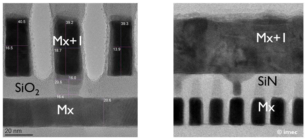
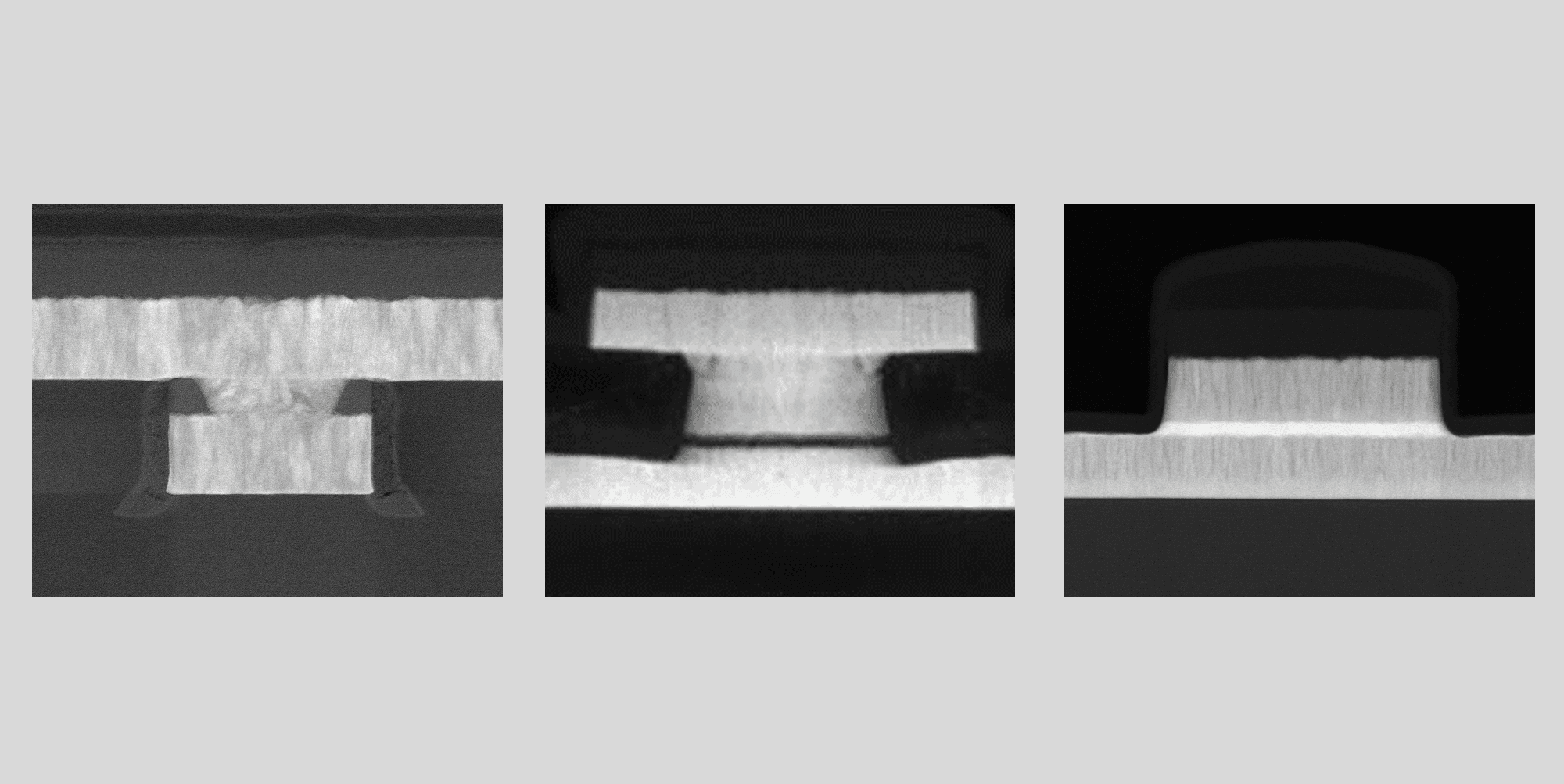
Bottom self-alignment was ensured by the selective removal of silicon nitride after gap fill, allowing the via to form on the confines of the lower metal line. The self-alignment towards the top metal layer (Ru) was achieved by the Ru over-etch step, applied after via overfill and Ru patterning.
Good resistance and reliability at 18nm pitch – the first-ever demonstration
Using a subtractive etch of Ru with fully self-aligned vias resulted in a functional two-metal level device at 18nm metal pitch. EUV lithography combined with self-aligned double patterning (SADP) was used for patterning the 9nm ‘wide’ Ru bottom local interconnect line (Mx), while single-exposure EUV lithography was used for printing the top line (Mx+1) and via. The top metal was combined with air gaps to counter the capacitance increase.
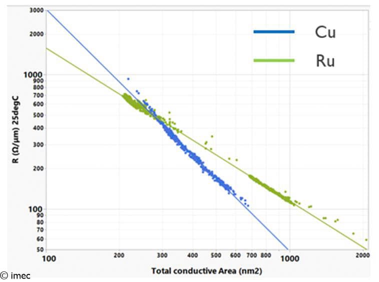
When benchmarking the line resistance vs. conducting area of Ru against Cu, Ru clearly outperforms Cu for the target metal pitches. Via self-alignment was confirmed both morphologically and electrically. Excellent via resistance was achieved (ranging between 40 and 60Ω for 26-18nm metal pitch), and a via-to-line breakdown field of >9MV/cm was demonstrated.
Zsolt Tokei: “We have demonstrated excellent values for all the key technical parameters, including via and line resistance and reliability. This demonstration shows that semi-damascene is a worthy alternative to dual-damascene for integrating the first three local interconnect layers of the 1nm technology node and beyond. Our two-metal-level device with fully self-aligned via has proven to be a key building block.”
Our demonstration shows that semi-damascene is a worthy alternative to dual-damascene for integrating the first three local interconnect layers of the 1nm technology node and beyond.
Further improvements are possible by increasing the aspect ratio of the lines (which reduces resistance) while keeping the air gaps (which keeps capacitance under control). At the same time, imec has concrete ideas for implementing middle-of-line (MOL) and BEOL technology boosters using the semi-damascene technology (which allows further area reduction at the standard cell level).
Want to know more?
- More details are described in the 2022 VLSI paper ‘First demonstration of two metal level semi-damascene interconnects with fully self-aligned vias at 18MP’, by G. Murdoch et al.
- ‘Logic technology scaling options for 2nm and beyond’, imec reading room.
- ‘A view on the logic technology roadmap’, imec reading room.
Authors

Gayle Murdoch
Gayle Murdoch graduated from the University of Edinburgh in 1997 with an honors degree in chemical physics. She began her career in the UK semiconductor manufacturing industry, first at NEC Semiconductors as a lithography engineer, and later joined Filtronic Compound Semiconductors, where she worked on etching development and integration for GaAs devices, eventually becoming a lead etch engineer. In 2008 she joined imec’s Advanced Lithography team before moving to BEOL integration in 2013. She has worked on a range of topics, including low k dielectric integration, fully self-aligned vias, and, most recently, semi-damascene integration. She currently holds the position of principal member of technical staff and leads the BEOL integration team

Zsolt Tokei
Zsolt Tokei is Distinguished Member of Technical Staff Interconnects at imec. He joined imec in 1999 and since then held various technical positions in the organization. First as a process engineer and researcher in the field of copper low-k interconnects, then he headed the metal section. Later he became principal scientist, Program Director Nano-Interconnects and, in 2016, was appointed Distinguished Member of Technical Staff Interconnect. He earned a M.S. (1994) in physics from the University Kossuth in Debrecen, Hungary. In the framework of a co-directed thesis between the Hungarian University Kossuth and the French University Aix Marseille-III, he obtained his PhD (1997) in physics and materials science. From 1998 he worked at the Max-Planck Institute of Düsseldorf, Germany, as a post-doctorate researcher. From the date of joining imec he continued working on a range of interconnect issues including scaling, metallization, electrical characterization, module integration, reliability and system aspects.
Discover more

A double world-first: integrating lithium niobate and lithium tantalate modulators on silicon photonics through micro-transfer printing
Read more
Imec demonstrates 16nm pitch Ru lines with record-low resistance obtained using a semi-damascene integration approach
Read more