Imaging technology development
Leverage imec’s longstanding expertise to develop image sensors with specifications outside those of commercial sensors.
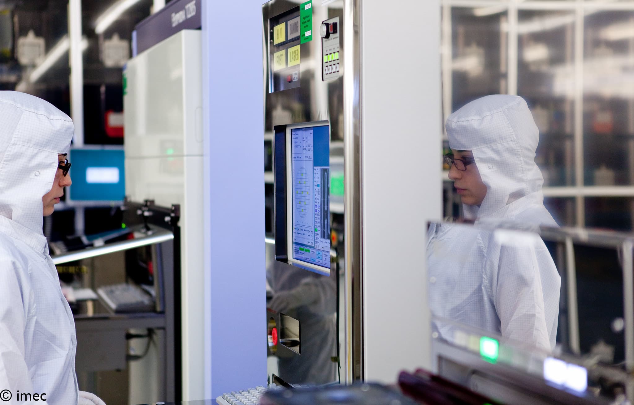
Imec’s specialty image sensors are based on CMOS image technology and tuned to meet exceptional specifications such as extreme speeds or ultra-low noise.
By combining this expertise with our heterogeneous integration processing platform, we can help you to develop and implement your ideas and concepts into a microsystem product. Prototyping and low-volume manufacturing of your dedicated high-end CMOS imagers and vision systems is achieved in-house on 200 and 300mm wafers. If needed, we can transfer the manufacturing process to a high-volume foundry.

White paper: monolithic microsystems
Elevate your application with advanced functionalities on top of CMOS
Imaging technology expertise
Imec’s imager activities are based on a 130nm CMOS process technology on 200mm silicon wafers, including a dual-gate module and MiM capacitors. Our baseline platform is extended with a number of imager-specific process modules:
- special epitaxial silicon wafers
- stitching for large area imagers
- CCD-in-CMOS process to combine the best of high-speed, low-power CMOS read-out circuitry with lowest noise, highest QE charge transfer domain CCD pixel technologies
- backside illumination with custom (ARC) anti-reflection coatings for maximal QE performance with possibility for tuning photon collection in UV, visible to NIR (near-infrared) wavelength range
- pixel-level Fresnel lenses
- hyperspectral filters
- organic photodiodes
Explore our imaging, sensing and actuation expertise
Tailored solution
We customize your imager according to your specifications, from design and development up to low volume manufacturing.
Choose up to which level you want to engage with imec:
- Design and develop your custom imager with imec, both at pixel and at imager system-on-chip level, including:
- fast and power-efficient column analog-to-digital convertors
- full imager architectural design including digital I/O
- Develop your custom imager including integrated filters:
- addition of 7 spectral filters to enable multispectral TDI
- post-processing of spectral filters on the wafer or on the glass lid
- Obtain ceramic-packaged imagers.
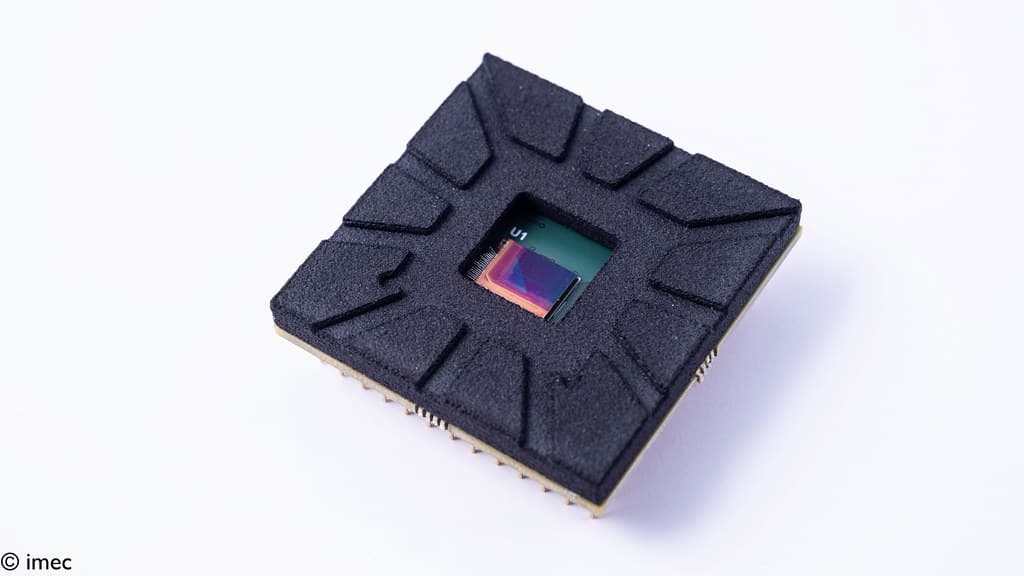
Examples of our imaging technology capabilities
CCD-in-CMOS for time delay integration (TDI) imaging
Imec’s CCD-embedded TDI CMOS image sensors combine the high level of integration and power efficiency of CMOS technology with low-noise, high-speed, spectrally-flexible CCD technology. Our CCD-in-CMOS technology combines single poly CCD photogates into a standard 130nm CMOS.
This technology is ideal for imaging scenes that move in a linear way:
- satellite-based earth observation
- drone-based earth observation
- industrial inspection
Ultra-high-speed imaging
Imec pushes the limits of fast imaging by maximizing the achievable frame rate. We realize this by leveraging a combination of:
- dedicated epitaxial silicon wafers
- backside illumination including backside bias
- state-of-the-art CMOS mixed analog/digital design
Backside-illuminated CMOS imagers feature very high intrinsic light sensitivity and are extremely efficient in detecting (near) ultraviolet and blue light.
Imec and Pharshighted: capturing reality at 326,000 frames per second
Lens-free microscope
Imec’s on-chip lens-free microscope offers large-field-of-view live imaging at micrometer resolution. It can be integrated into life sciences and biotech tools, targeting multiple applications such as label-free cell monitoring, automated cell culturing, or automated high-throughput microscopy.
Hyperspectral imaging
Imec has developed a process for depositing hyperspectral filters directly on top of CMOS image sensors at wafer level. The combination of the production of filters and sensors in one CMOS-compatible flow, leads to an overall simplification and cost reduction, and enables mass production.
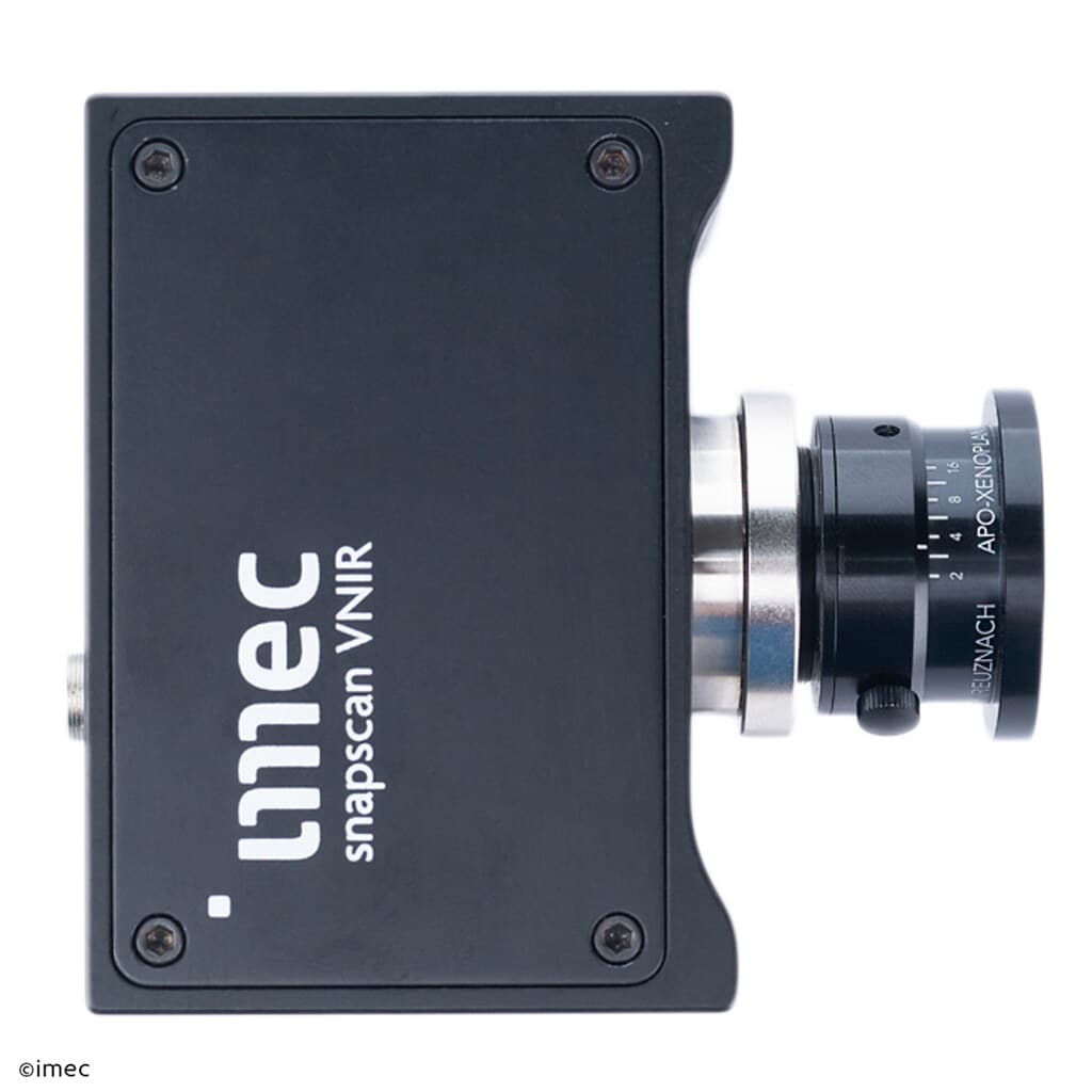
Imaging technology prototypes
We’ve developed several prototypes of TDI imagers using our CCD-in-CMOS technology:
Analog output TDI imagers
Spec | Value |
Array size | 512 stages x 1024 columns |
Pixel size | 5µm |
Stage selection | 8 or 512 |
Full well | 18ke- |
Noise | 20e- |
Conversion gain | 25µV/e- |
Dark current | 3nA/cm2 |
CTE | >99.995 at 400kHz |
Supply voltages | 3.3V, 1.2V and -1.5V |
Digital output TDI imagers
Spec Target | Value |
Array size | 4k x 256 per band |
Pixel size | 5.4µm |
Stage selection | 1-to-256 per band individually |
Bi-directional | Yes |
Number of bands | 1 band or 7 bands #bands can be enabled |
Line rate | Up to 300kHz aggregate (e.g. 57kHz per band when all bands enabled) |
Power | <5W |
Dynamic range | >60dB – 40dB |
CTE | >0.99995 at >300kHz |
QE | >90% VIS /wo color filters >60% UV |
Package type | Ceramic µPGA |
Output type | 32x 1Gb/s LVDS |
Color filters | On glass lid or on the sensor |
Multispectral TDI imager
We have developed a color or multispectral TDI imager based on our 7-band digital TDI. This is particularly interesting for airborne remote sensing, satellite imagery, life sciences instrumentation and machine vision applications.
Want to tap into out expertise and infrastructure to develop your dedicated image sensor?
Some examples of what we have done
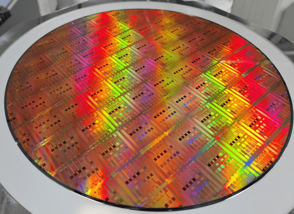
Imec successfully integrates colloidal quantum dot photodiodes (QDPDs) on metasurfaces developed on 300mm CMOS wafers
Pioneering approach makes compact, cost-effective, high-resolution multispectral shortwave infrared (SWIR) sensors accessible, enabling broad application in security, agriculture, automotive, aerospace, and more.
Read moreWhite paper: monolithic microsystems
Learn how to elevate your application to new heights with advanced functionalities on top of CMOS.
Read more
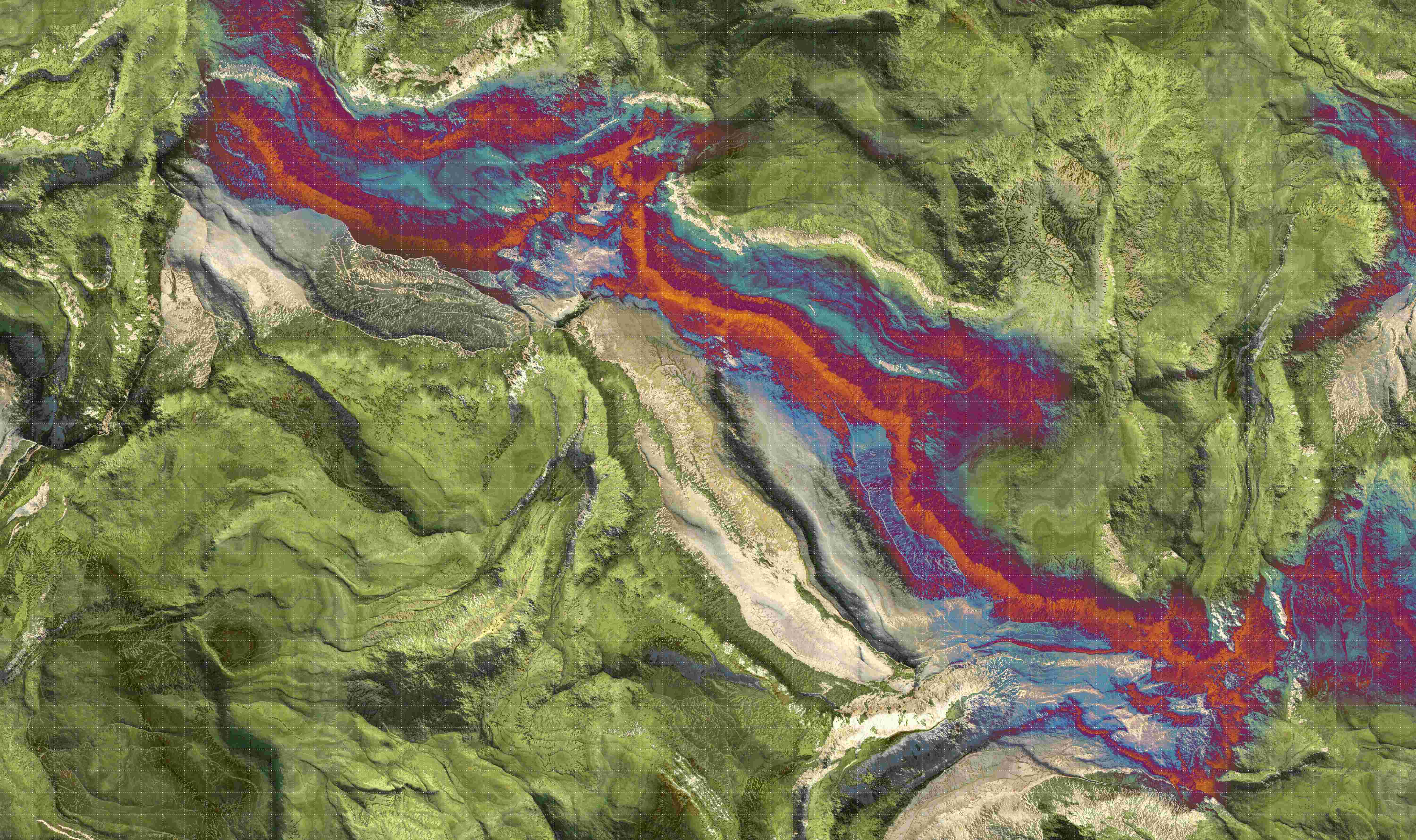
Imec hyperspectral sensor aboard newly launched earth-observation satellite
The IPERLITE mission is designed to demonstrate next-generation hyperspectral imaging technology in space. At the core is a hyperspectral sensor developed by imec.
Read more