Nano-optics
Want to integrate nanoscale optical components in your innovative products such as cameras, displays or sensor systems? Imec helps you with the full development process.
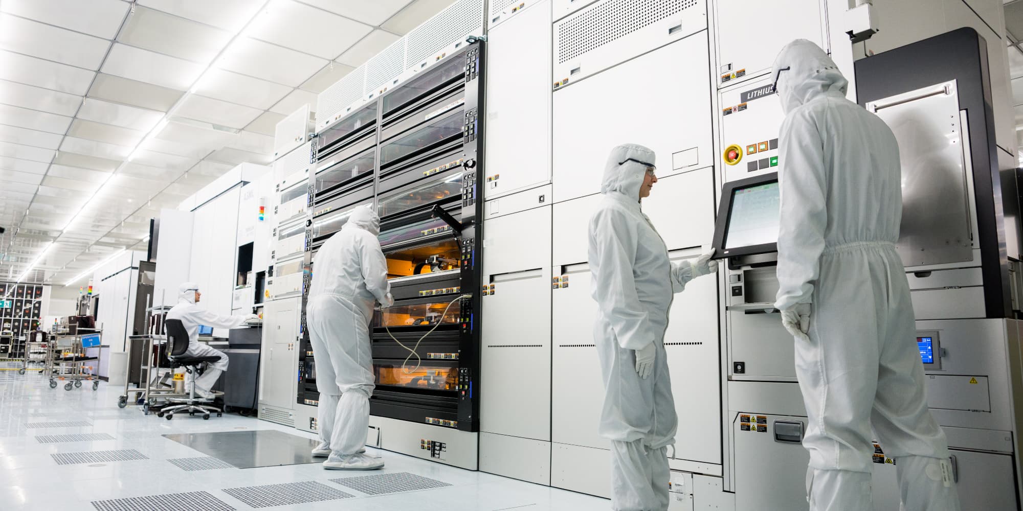
For centuries, optical instruments remained bulky and expensive. They were produced by refining mechanical parts, usually in glass, that manipulate the light in order to sense, measure, make projections, ...
It’s only recently that there’s an alternative for this traditional approach: nano-optics delves into the toolbox of the semiconductor industry. The idea is to create nanostructures that fulfill optical functions. Examples of such functions are focusing and color splitting – at a wavelength scale and with visible as well as infra-red light.
Want to dive into this toolbox? Imec is ready to help youwith the development and integration of such nano-optics components in its state-of-the art cleanrooms. And we can guide you towards large-scale manufacturing.
Advantages of nano-optics
The main advantage of nano-optics? Its compactness compared to traditional macro-optics. Moreover, nano-optics (or flat optics) components are processed using well-established techniques from the microchip industry, such as lithography and thin-film deposition. The result is that manufacturing becomes cheaper and easier to upscale.
Some other advantages of nano-optics are:
- They exhibit high design flexibility and material flexibility.
- They can be perfectly alignmed and optimized at pixel level.
- They're compatible with further post processing on complex integrated circuits.
Applications
The miniaturization of optical components enables their integration into complex systems-on-chip. This opens the door to product innovations in markets such as:
- cameras: 3D, light pipes, spectral imaging, ...
- displays: directive, 3D, microLEDs, ...
- glasses: mirrors, diffusers, scatters, ...
- sensors: spectrometers-on-chip, fluorescence imaging, sorting, ...
Develop your nano-optics components with imec
At imec, we support the full development of flat optics components such as filters, polarizers and lenses. Based on your requests, we:
- Assess the feasibility of your flat optics component.
- Design the component and develop the process.
- Realize a first prototype.
- Optimize the design and process technology
In our 200- and 300-mm cleanrooms, we're able to:
- Process on glass for standalone applications.
- Post-process on top of device wafers for integrated applications.
Imec not only helps you to address technological challenges. Thanks to our thorough knowledge of the industry, we function as your full-fledged strategic partner – right down to venturing support.
Click the button below to get in touch.
Read more
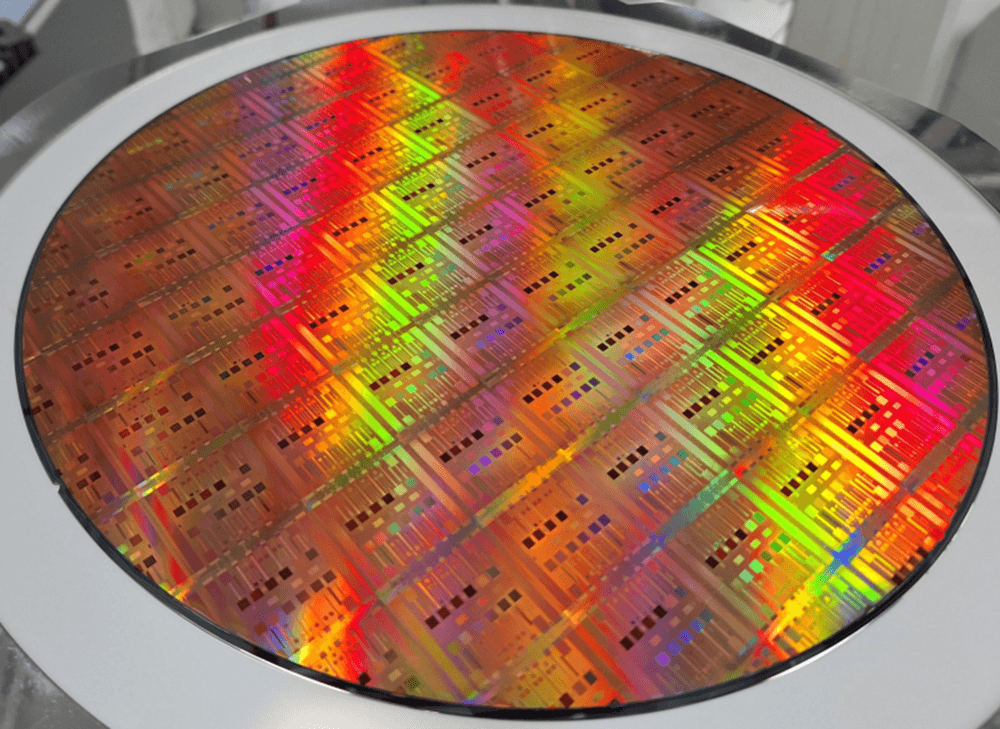
Imec successfully integrates colloidal quantum dot photodiodes (QDPDs) on metasurfaces developed on 300mm CMOS wafers
Pioneering approach makes compact, cost-effective, high-resolution multispectral shortwave infrared (SWIR) sensors accessible, enabling broad application in security, agriculture, automotive, aerospace, and more.
Read more
White paper: monolithic microsystems
Learn how to elevate your application to new heights with advanced functionalities on top of CMOS.
Read more

Imec hyperspectral sensor aboard newly launched earth-observation satellite
The IPERLITE mission is designed to demonstrate next-generation hyperspectral imaging technology in space. At the core is a hyperspectral sensor developed by imec.
Read more