Custom chip manufacturing
Go from idea to scalable and reliable semiconductor manufacturing with IC-Link.

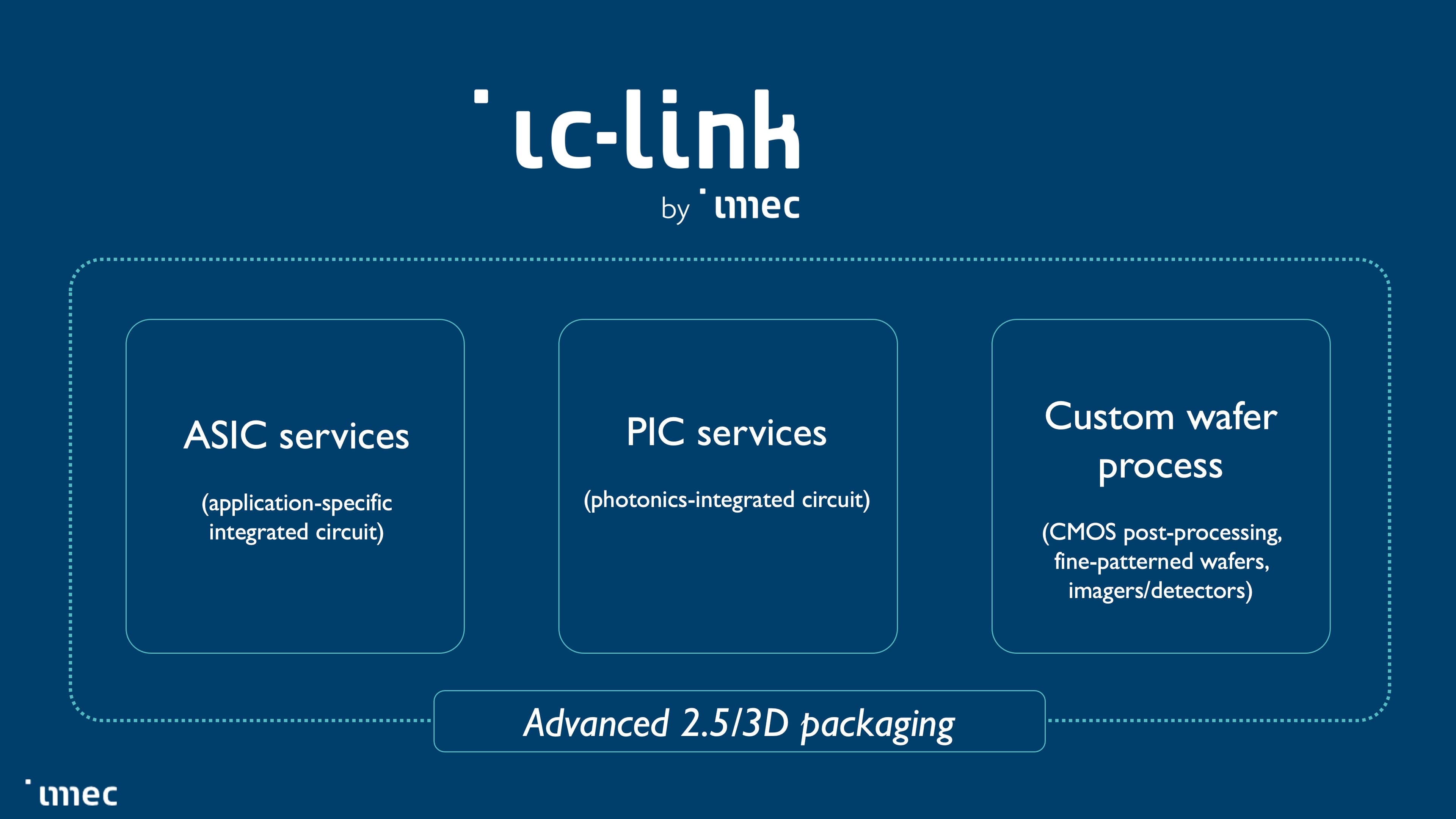
IC-Link provides customized solutions for innovative chip manufacturing, built on imec’s semiconductor expertise. Next to silicon production, the division includes services spanning from design through packaging, assembly, qualification, and supply chain management.
Technologies range from ASICs in CMOS, including the most advanced commercially available nodes, to imec-developed integrated photonics, custom wafer processes, and 2.5D and 3D packaging. This portfolio continually expands with new platforms fresh from R&D once they are commercially validated.
ASIC services
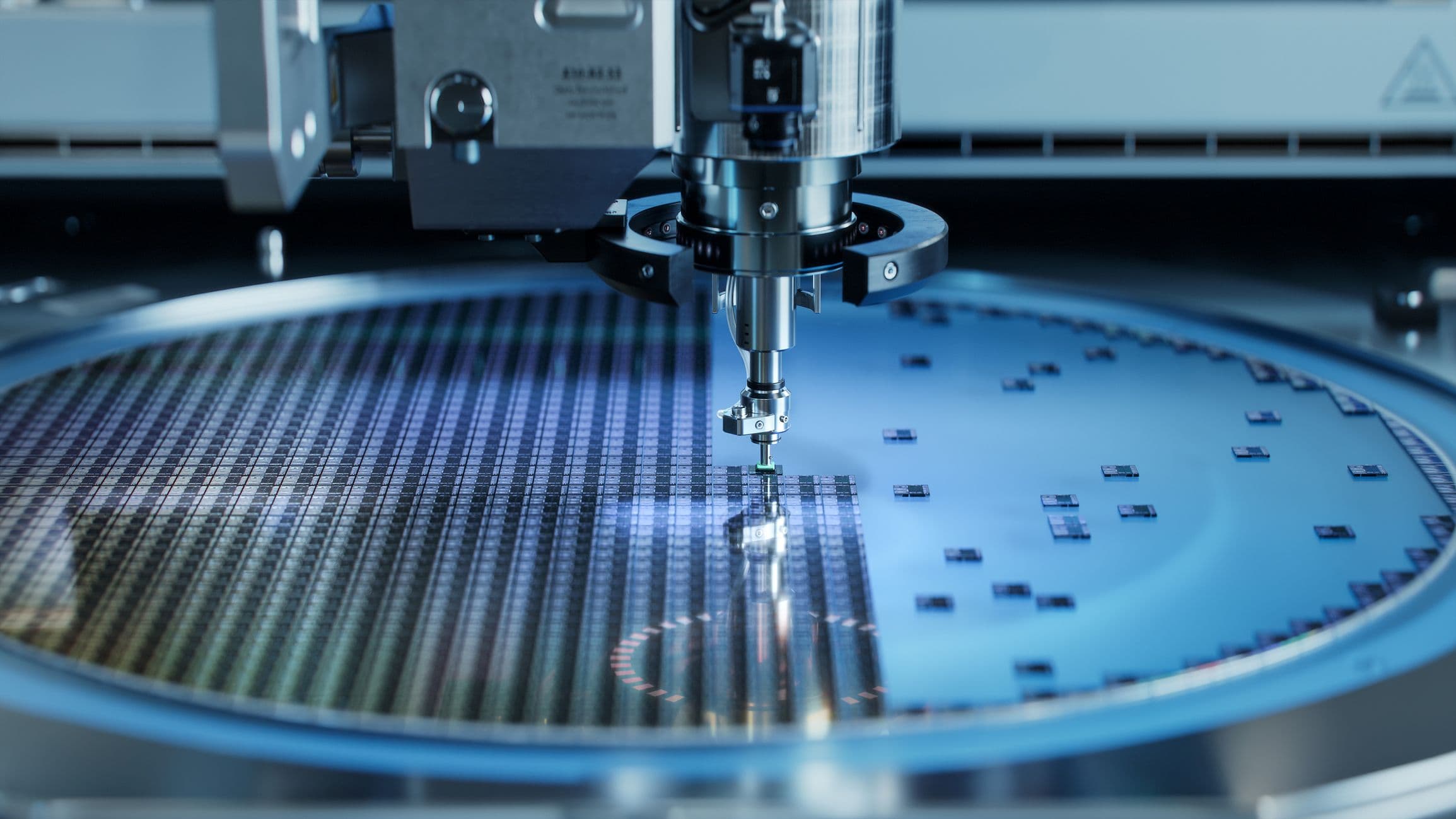
A custom ASIC allows you to differentiate your product through higher performance, smaller form factor, better IP protection, and more.
IC-Link’s CMOS ASIC offering includes:
- A wide range of technology nodes down to N2
- Partnerships with commercial foundries, including TSMC as Value Chain Alliance (VCA) member
- Flexible business models including full turnkey
- Design capabilities across digital, analog and mixed signal
- Packaging solutions including 2.5D/3D design and production
- Testing development, qualification and supply chain management services to serve high-volume customers
PIC services
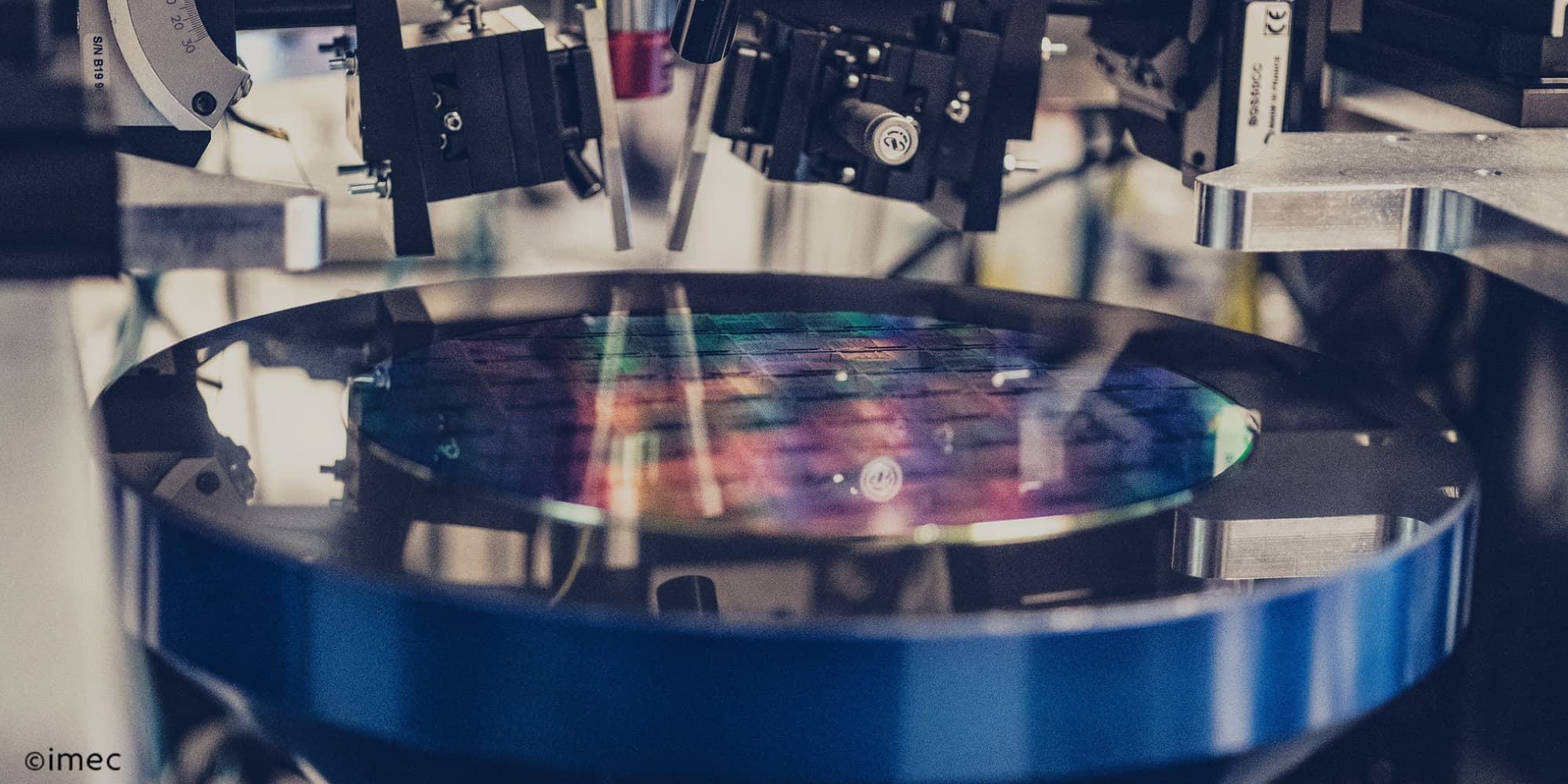
Differentiate your application by harnessing the high performance and low power consumption of a silicon photonics integrated circuit (PIC).
IC-Link's 200mm silicon photonics platform, iSiPP200 offering includes:
- A complete, state-of-the-art PDK, regularly updated with new advancements, coming from imec’s leading photonics research program
- Flexible volumes thanks to foundry access
- Service model to go from idea to production
- Additional photonics platforms on the roadmap
Custom wafer process services
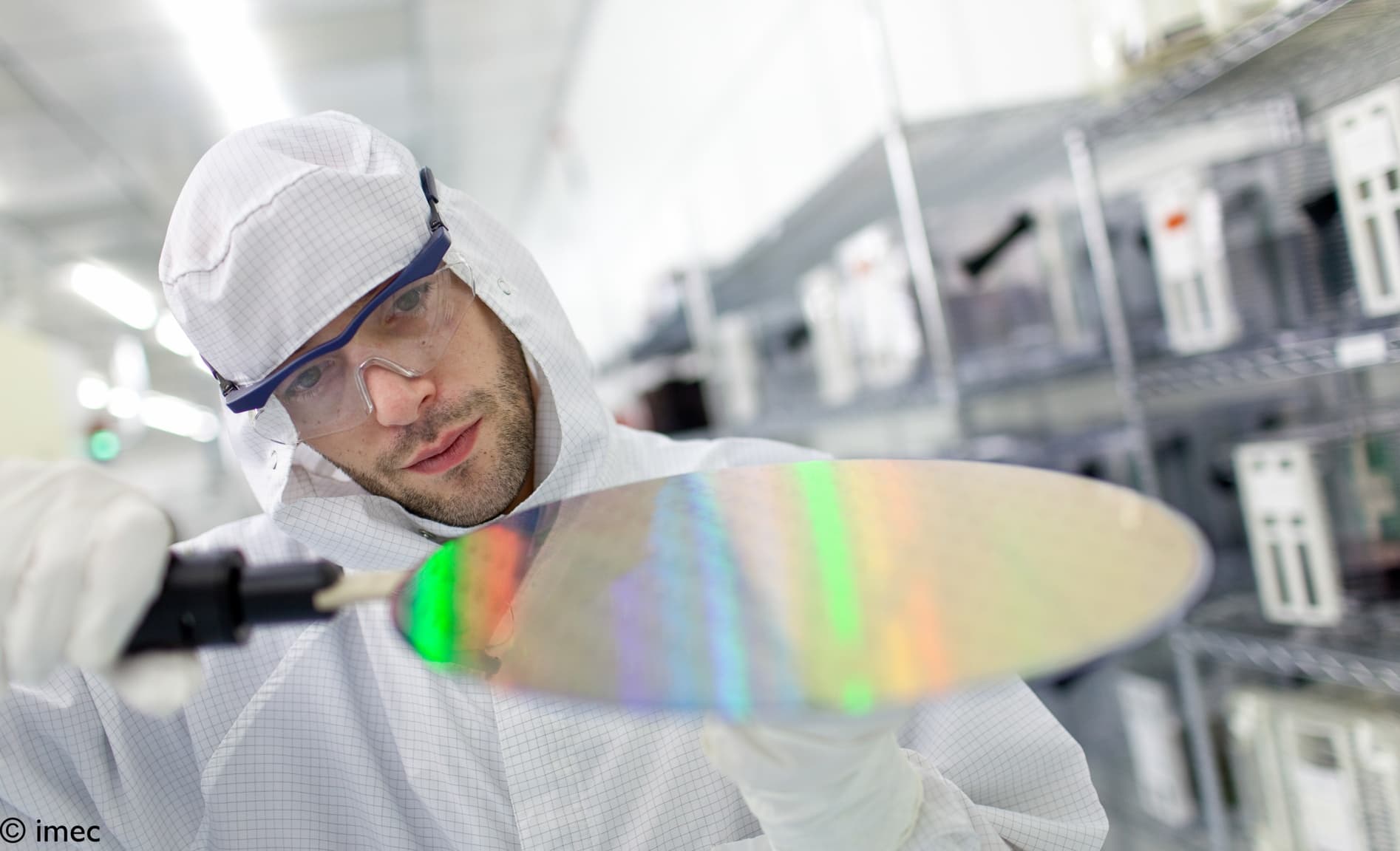
Get access to manufacturing capabilities without a standard flow. These include:
- Custom-developed imagers and detectors, from design to production based on imec’s R&D
- Fine-resolution wafers using state-of-the-art lithography tools
- CMOS post-processing: unique capabilities that can be combined with photonics, advanced lithography, and more
Example project: From circuit design and specialty Si-processing to seeing atoms
Advanced packaging services
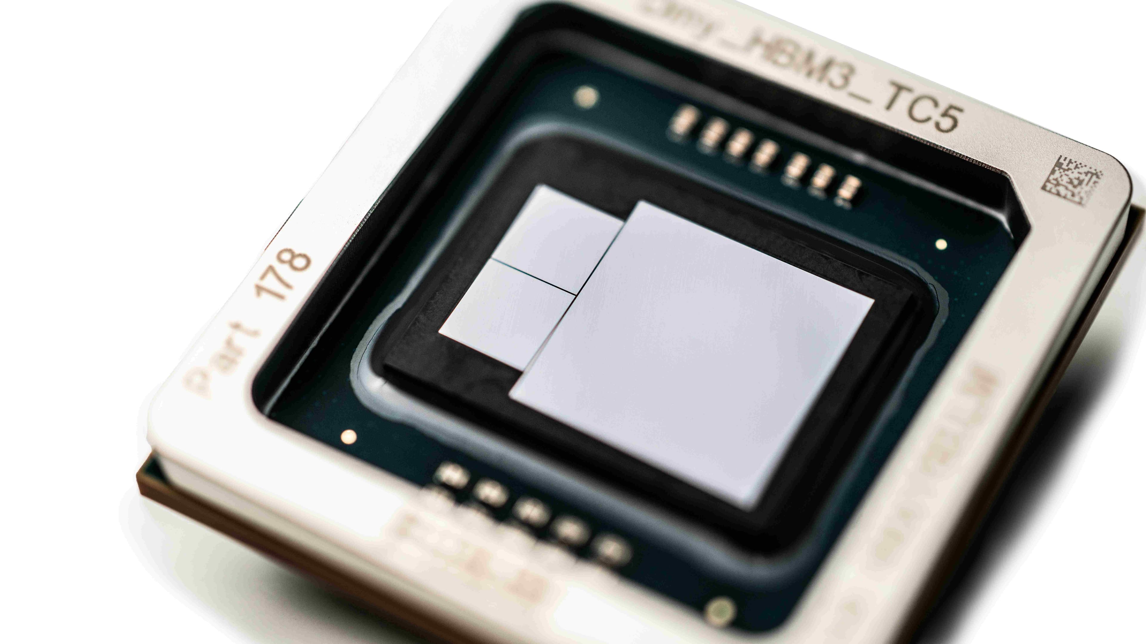
A broad range of mainstream to advanced packaging techniques is available through our ASIC partners. This is complemented by selected imec-developed 2.5D and 3D packaging services.
Examples include:
- 2D packaging: ball grid array (BGA), land grid array (LGA), wafer-level chip-scale packaging (WLSCP), multi-chip module (MCM), system in package (SiP)
- 2.5 packaging: via packaging partners, imec-developed solution coming in 2026
- 3D packaging: via packaging partners, imec solution under development
Newsroom

Subscribe to our thematic newsletters