
Your access to innovative chip manufacturing
Turn bold ideas into silicon with IC-Link’s custom chip manufacturing services, backed by imec’s world-leading R&D.

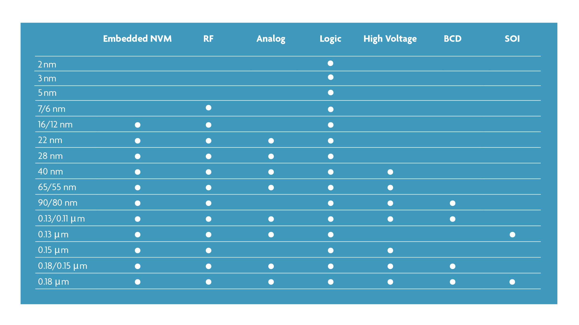
Process technology selection
The starting point for any design is selecting the right process technology node for the manufacturing of your chip.
Our skilled IC-Link team helps you make the technology choice that best fits your technical and market requirements. And subsequently provides you with the corresponding design kit and cell libraries so you can create your chip layout.

Your practical guide to ASICs
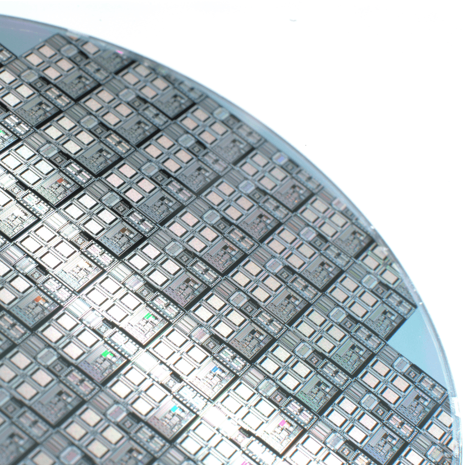
ASIC manufacturing in CMOS
As a leading TSMC Value Chain Alliance (VCA) member, imec offers you access to an extensive range of mature and cutting-edge technologies. And as a main partner of Europractice we also support technologies from other foundries, such as X-FAB and UMC. Along with the variety of technologies, you can choose from a range of options – including FinFET logic, embedded memory, and mixed signal.
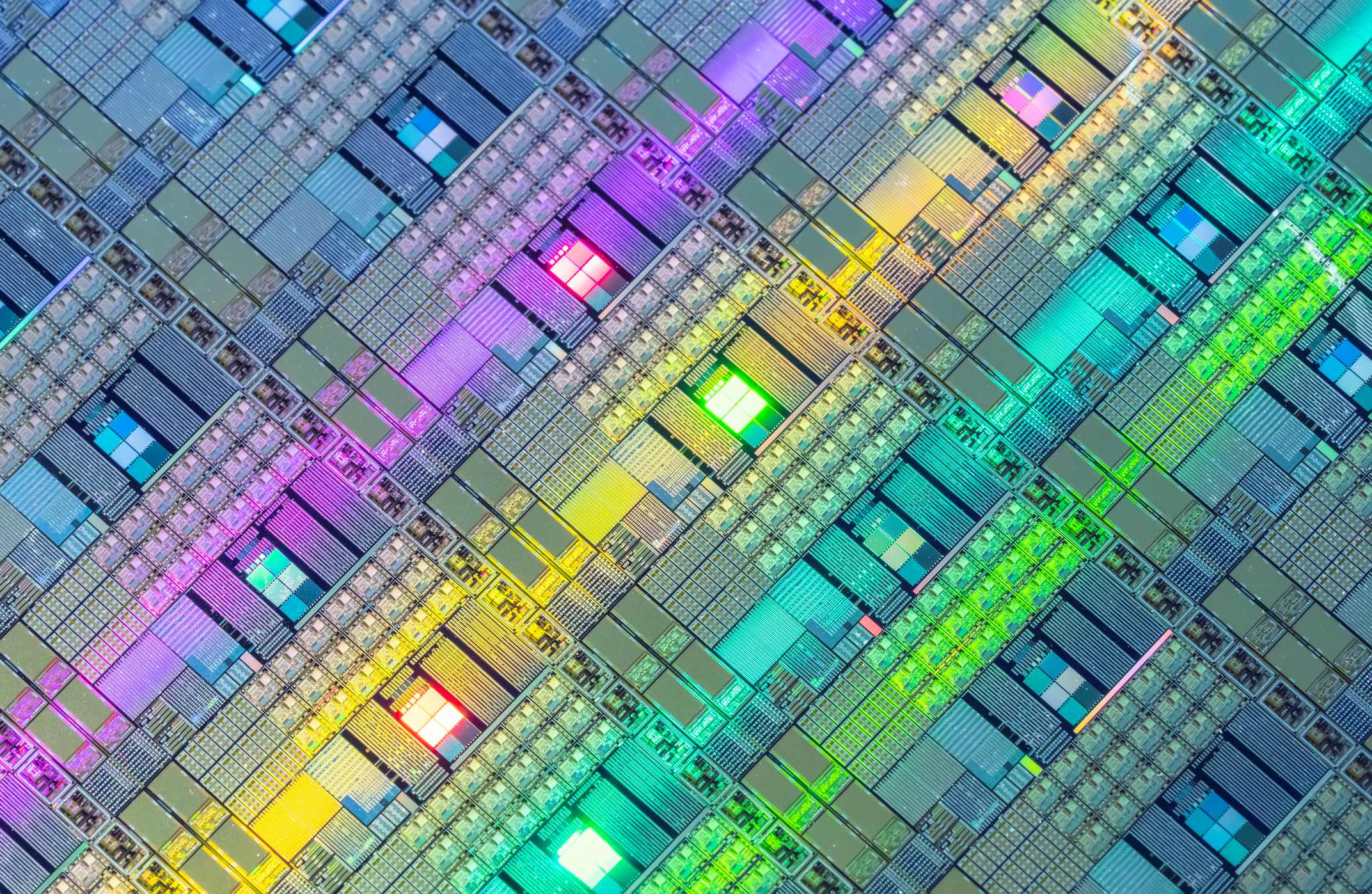
Silicon photonics
Leveraging the leading imec-developed photonics platform, IC-Link offers silicon (Si)-based photonic integrated circuit (PIC) fabrication from PDK to volume production. Our Si-based process is optimized for applications such as data center interconnects and high-speed transceivers with a large active component library.

Custom wafer processes
IC-Link offers access to manufacturing capabilities that do not have a standard flow, such as:
- Custom-developed imagers and detectors, incorporating the latest imec research.
- Fine-resolution wafers using state-of-the-art lithography tools. The wide offering includes special coatings and glass substrates.
- CMOS post-processing: unique capabilities that can be combined with photonics, advanced lithography, etc.
Work with us
Want to discuss your chip manufacturing needs? Don’t hesitate to get in touch.