ASIC manufacturing in CMOS
End-to-end ASIC solutions in mature to advanced nodes
Turnkey ASIC manufacturing for prototyping and high-volume production
IC-Link delivers a complete, flexible pathway to custom ASIC development—from concept to qualified silicon.
We leverage imec’s deep semiconductor R&D heritage and our membership in the TSMC Value Chain Alliance (VCA) to offer unparalleled access to the most advanced CMOS process technologies and a global ecosystem of design, manufacturing, and packaging partners.
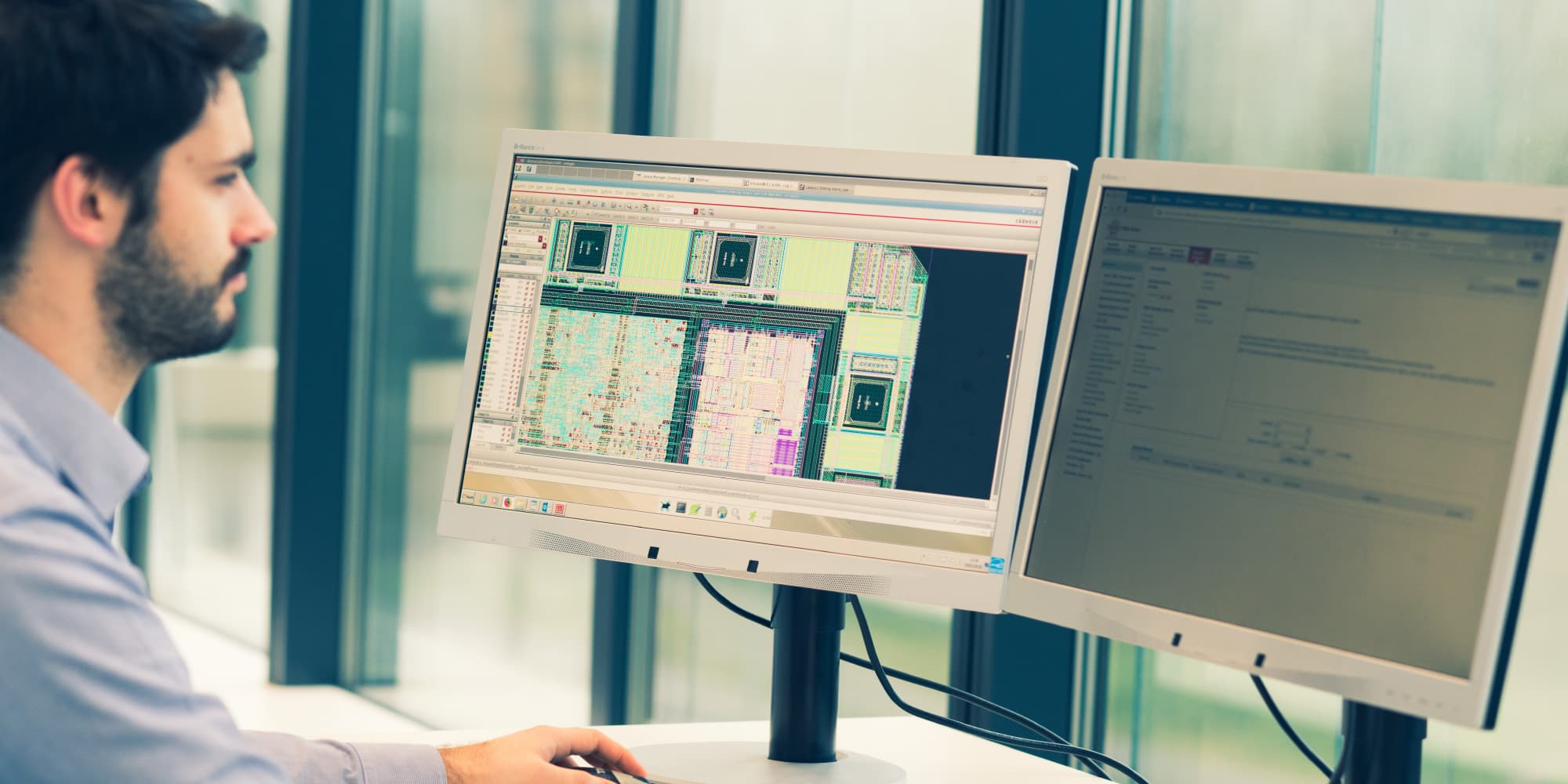
Flexible engagement models for custom ASIC development
Whether you need a turnkey ASIC or a flexible engagement model, IC-Link provides the expertise and infrastructure to accelerate your design to production.
Our services span all stages of the ASIC lifecycle: specification, design enablement, foundry interface, wafer manufacturing, packaging, testing, and volume ramp.
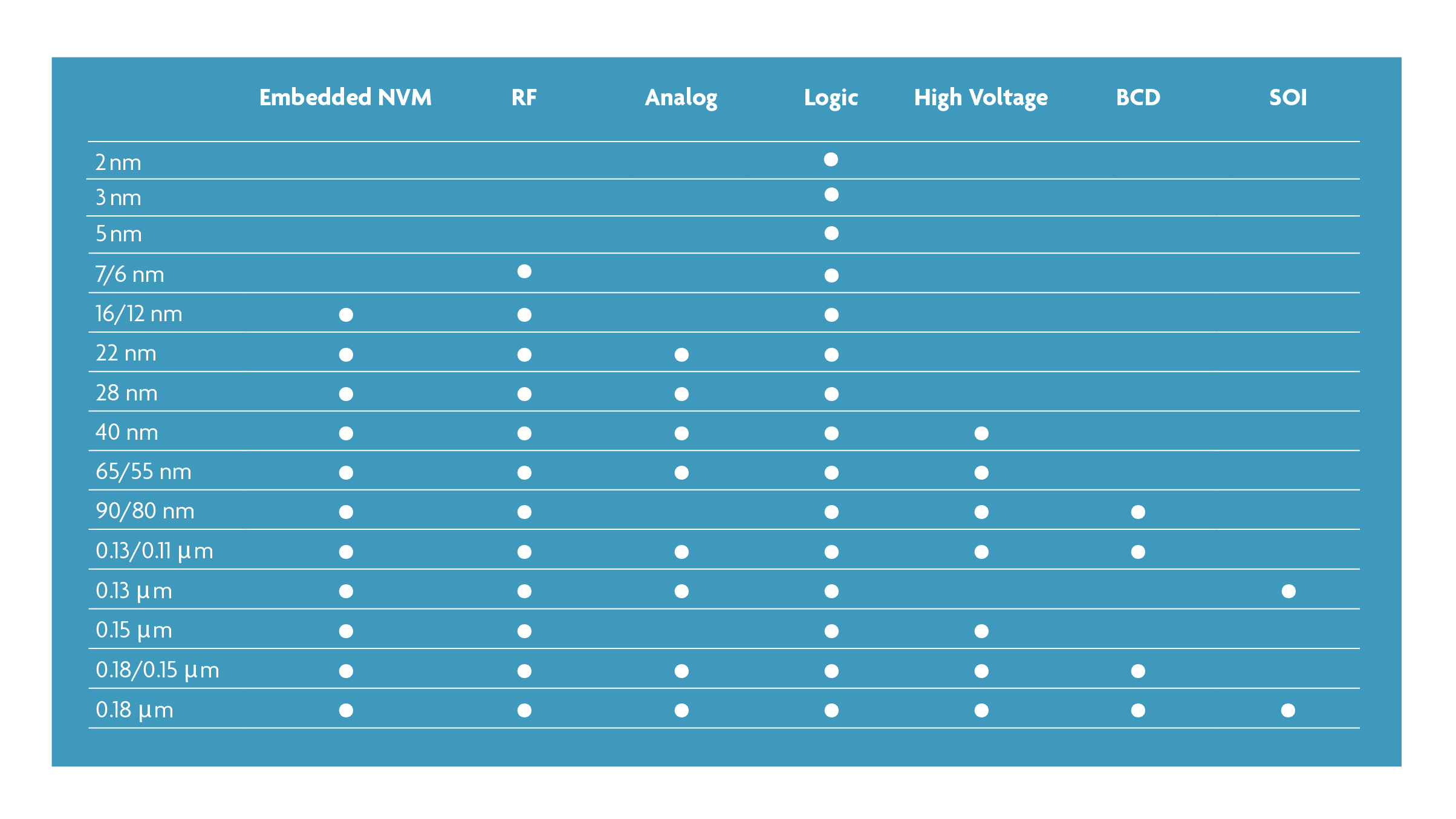
Advanced and mature CMOS process nodes
Our close collaboration with TSMC and other commercial foundries enables our customers to gain early access to advanced process nodes—down to single-digit-nanometer CMOS logic technologies—along with a complete portfolio of wafer technologies, including mixed-signal, RF, high-voltage, and embedded memory options.
For cost-sensitive or specialized applications, we also support mature nodes optimized for power, performance, and reliability.
Scalable manufacturing and supply chain management
IC-Link’s scalable manufacturing model ensures seamless migration from prototype to high-volume production, with quality control and supply-chain management handled through imec’s established foundry relationships.
Regardless of the target end-market, ASIC customers benefit from imec’s decades of experience in scaling CMOS technologies and our deep understanding of design-for-manufacturability.
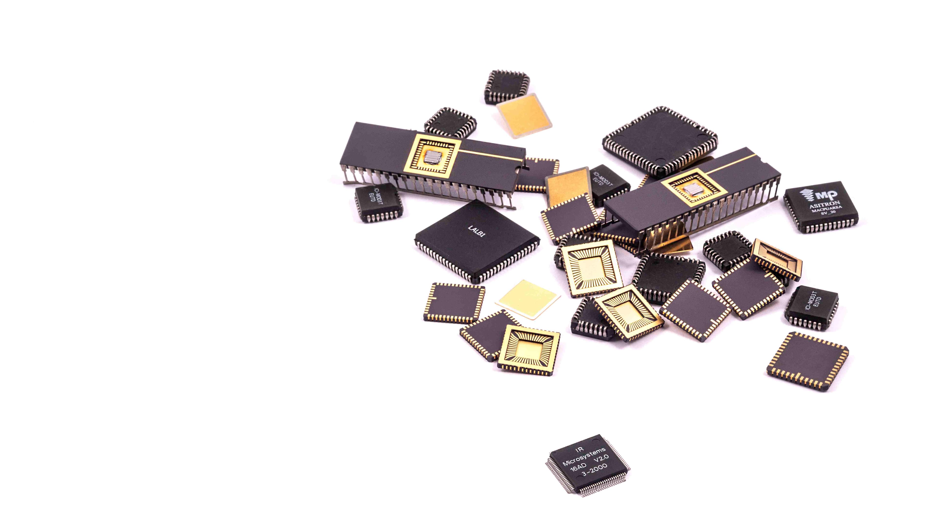
Accelerated ASIC innovation from lab to market
By bridging the gap between research, innovation and commercialization, IC-Link enables companies of all sizes to bring differentiated semiconductor solutions to market faster, at lower risk, and with the backing of one of the world’s most trusted names in nanoelectronics.
A selection of our ASIC development projects:
- Nanopower Semiconductor – Extending IoT device battery life
- FemtoAI – Low-power AI noise reduction
- A shared journey: Frontgrade Gaisler and IC-Link
- The Six Semiconductor – 7nm chips with 2.5D integration
- Raspberry Pi – An affordable and accessible microcontroller
IC-Link: Turning your ASIC vision into silicon reality.
Reading room