Thermo Fisher Scientific – A unique custom chip for electron microscopy
27/01/2026
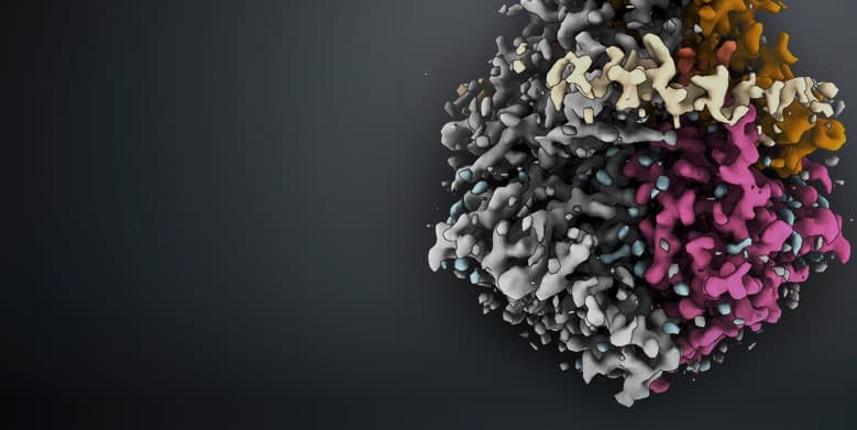
3D molecular structure rendered in gray, magenta, and orange against a dark background

Off-the-shelf sensors work perfectly well for smartphone cameras. But a tool that must visualize structures at atomic-level resolution requires a highly customized sensor chip. That custom chip can only come from imec and IC-Link, says Olivier Rainaut, senior director of R&D for life science electron microscopy activities at Thermo Fisher Scientific.

Electron microscopes don’t use light but electrons to visualize a sample. The sensor capturing these electrons must be extremely sensitive to allow the analysis of life-science images with exceptionally low contrast, such as tissues, membranes, and proteins.

In addition, the remarkable size of the chip (5 × 5 cm, or 4 dies on one wafer) brings added challenges in terms of design, packaging, and dicing.

Thermo Fisher Scientific has been working on these custom sensors with imec (for the research) and IC-Link (for full development and manufacturing) for more than ten years. This collaboration has already resulted in four commercialized design iterations. New developments are on the way, while the production yield of existing products continues to be optimized.

For Olivier, the value of this long‑term collaboration lies in having guaranteed access to a partner capable of meeting the required specifications for design quality, volume, and yield.

Discover more

Engineer reviewing chip design layouts on multiple monitors

IC-Link selected as a European Design Enablement Team (DET) under EuroCDP

26/05/2026
Read more
3D rendering of stacked semiconductor chips and solder bumps for advanced packaging

IC-Link joins TSMC 3DFabric® Alliance

12/05/2026
press release
Read more
Futuristic data center corridor lined with server racks and blue lighting

IC-Link’s role in Celestial AI’s journey

07/04/2026
Read more
Close-up of a semiconductor wafer with a blue and purple patterned photonics grid

IC-Link now also offers silicon nitride (SiN) manufacturing services through imec’s mature platform

19/03/2026
Read more
AI chip connected to multiple smaller processor blocks by glowing data lines

ASIC vs GPU for AI

27/04/2026
Read more
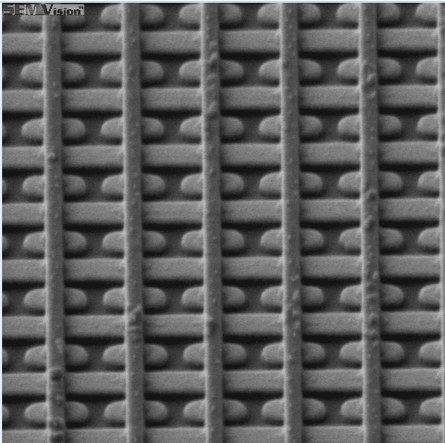
Scanning electron microscope view of a high-density electrode array

Next-generation, permanent DNA-based data storage for the AI age

05/03/2026
press release
Venturing
Read more
Silicon wafer with colorful chip patterns inside semiconductor equipment

Teradyne – using ASICs to build a competitive advantage

27/01/2026
Read more
Glowing secure chip illustration on a dark circuit board

Fortaegis – Developing the world’s most secure high-performance chip

19/01/2026
Read more
Colorful integrated photonics chip layout with diagonal rows of square and rectangular circuit patterns

A close look at iSiPP200, IC-Link’s integrated photonics platform

30/09/2025
Read more