
IC-Link by imec
Customized solutions for innovative chip manufacturing
Streamline and accelerate your path from concept to production.
ASIC and photonic IC manufacturing
Turning an idea into silicon shouldn’t be limited by access, complexity, or scale. With more than four decades of experience, IC-Link makes it possible for companies of any size—from startups to global innovators—to bring their devices to life.
Through our extensive foundry network and technical infrastructure, we provide fast, reliable access to our end-to-end ASIC and integrated photonic IC (PIC) services.
In addition to ASICs and PICs, we offer access to custom wafer manufacturing processes, resulting in imagers and detectors, fine-resolution wafers, and CMOS post-processing implementations.
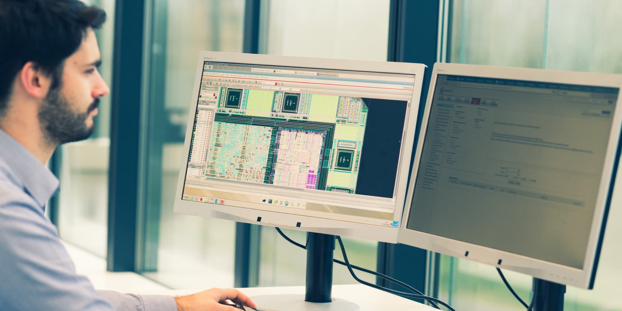
Flexible engagement across the semiconductor value chain
You can engage with us across the entire semiconductor value chain—from design, IP selection and manufacturing, to advanced packaging, testing and qualification, and supply chain management—choosing between multi-project wafer (MPW) runs for cost-effective prototyping and dedicated full-mask production for volume scaling.
IC-Link manages the full design-to-manufacturing flow, ensuring each step meets your performance, yield, and reliability targets.
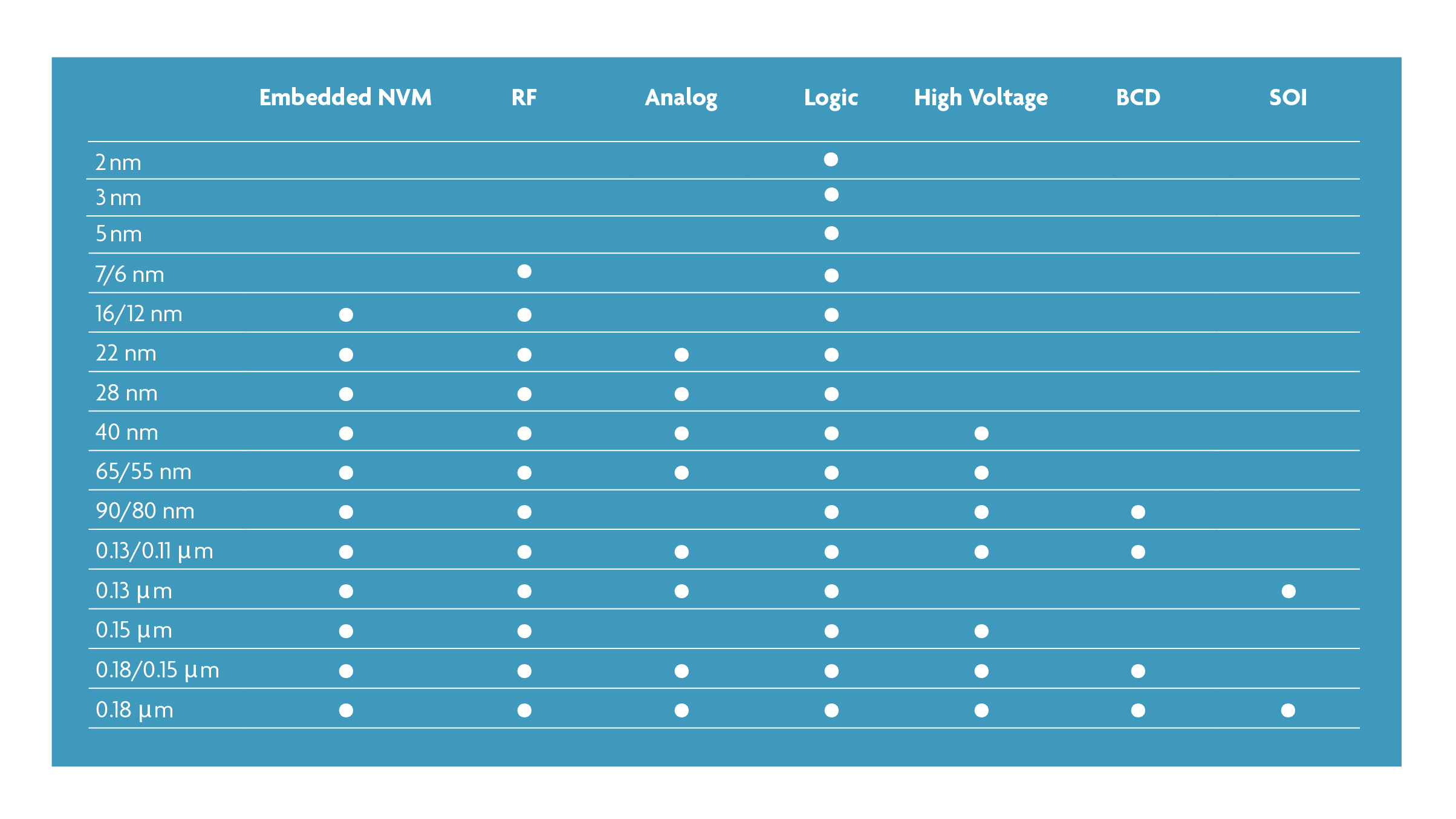
ASIC Development from design enablement to production
For ASIC development, we support a range of geometries, from mature through advanced CMOS nodes, along with design enablement resources that include verified process design kits (PDKs), foundry-qualified IP, and a host of advanced packaging options.
Turnkey and COT models for scalable IC manufacturing
IC-Link’s flexible business models accommodate varying project scales and budgets, whether you own your own tooling (COT) and are looking for a reliable wafer supply, or require our low-risk full-turnkey (FTK) model, where we manage the entire production process so that you can focus on your core business.
Each model provides cost control, IP security, and supply-chain facilitation.
Proven path from design to silicon
By combining proven process expertise, foundry relationships, and engineering infrastructure, IC-Link enables faster tape-out cycles, higher first-time-right success rates, and smoother transitions from R&D to production.
IC-Link by imec — Your complete path from design to silicon, backed by world-class technology access and integration.
Reading room