Capturing reality at 326,000 frames per second
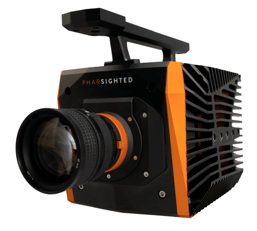
The Pharsighted E9•100S is the world’s most light-sensitive ultra-high-speed camera. Its image sensor is developed and manufactured by imec.

Does a galloping horse ever have its four hooves off the ground? That question was the source of a significant controversy in the late nineteenth century. Until in 1878, Eadweard Muybridge settled the matter with his sequence of iconic pictures that’s sometimes named the first ‘animated gif’.

We can consider Muybridge’s accomplishment as the beginning of high-speed imaging. Although that field has evolved a lot, its primary purpose remains the same: to improve our understanding of how the world functions by capturing images at the highest possible speed. Present-day applications include the hyper-detailed analysis of manufacturing processes, particle movements, fluid dynamics, drop and crash impacts, and so on.
‘High speed’ meant 12 frames per second in Muybridge’s time. Today, the world’s most light-sensitive ultra-high-speed camera – the Pharsighted E9•100S – reaches 326,000 frames per second (full frame: 640x480 pixels) and up to 2,720,000 frames per second at lower frame size (640x32 pixels). The outstanding light sensitivity is ISO 160,000 (monochrome).
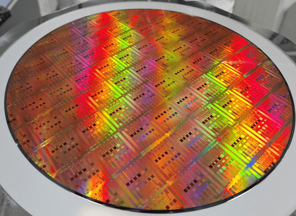
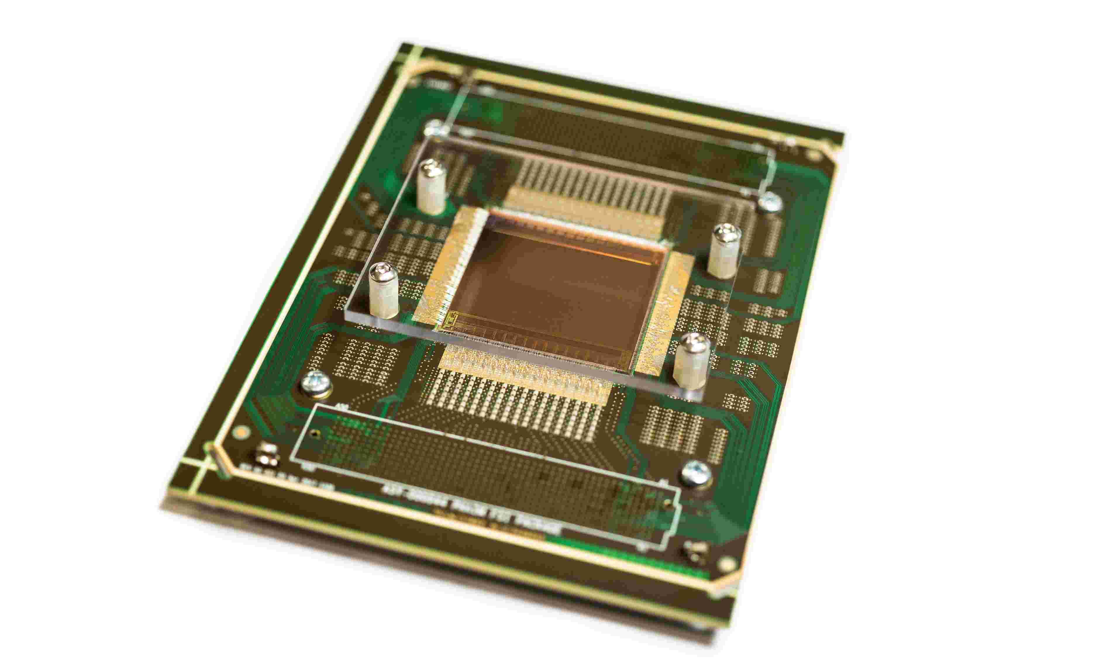
Such an astounding performance is primarily enabled by the backside-illuminated CMOS imager inside the E9•100S. For developing and manufacturing this crucial component, Pharsighted partners with imec.
Unique combination of capabilities
For Phil Jantzen, Pharsighted’s founder, the choice for imec was a no-brainer: “Only imec could deliver the specifications we need for this imaging chip. Even though you can find some of the skills elsewhere, the combination of those skills is unique to imec.”
This doesn’t mean this sensor is something imec can just pick off the shelf. Paul Goetschalckx, program and department director of imagers design and test at imec: “This imaging chip is an excellent example of design-and-manufacturing-on-demand projects that imec undertakes to serve specific needs in niche markets. Such projects always come with great challenges. In this case, a.o. the task of combining a large pixel area with high imaging speeds, including a massive output data rate.”
Tailored process, pixel and circuit design
The innovations needed for this project fall into two categories:
- Imec developed a CMOS imagerprocess that’s dedicated to high-speed imaging.
- Imec developed dedicated pixel and readout circuits integrated on a single die to output digital image data at high speed.
The Pharsighted E9•100S is a feat of engineering and a highly specialized piece of equipment. Needless to say, it doesn’t come off the assembly line by the thousands. Imec serves Pharsighted by managing the sensor supply chain from silicon processing to delivery, including testing.
Looking forward
The Pharsighted E9•80S hit the market in 2022 and is rapidly gaining interest with companies that need visualization capabilities that exceed 100,000 frames per second. For imec, the work is far from done. “We’re looking towards future generations of this high-speed imager chip,” says Paul Goetschalckx.
It's about more than technical capabilities. “Pharsighted is constantly pushing to break barriers that were believed to be rock solid,” says Phil Jantzen. At imec, they have that same mindset. It’s a key reason why this collaboration is so successful.”
Want to discuss your challenge in the imaging space?