Why biotech innovators choose imec for their custom silicon
PacBio and Twist Bioscience share why they partnered with imec to advance their product roadmaps.

In short
Imec’s technology platforms and process capabilities are available for biotech innovators to fabricate unique, monolithically integrated, high-performance systems. In this article, PacBio and Twist Bioscience talk about their partnership with imec, explaining how imec combines the flexibility of a university fab with the professionalism and standards of a foundry.
Silicon, the silent engine driving biotech roadmaps
Besides advances in chemistry, it was semiconductor fabrication technologies that brought the cost of sequencing drastically down from a million dollar per genome to 100 dollars today. They did this by enabling higher-density reads and massive parallelization through nanowell patterning, field-effect transistor (FET)-based sensors, photonic integrated circuits, and CMOS-based image sensors.
Imec’s collaborative innovations with industry
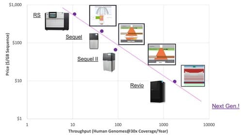
One of the leading companies in third-generation (long-read) sequencing technologies is PacBio. Their approach is based on repeated sequencing of long reads to effectively normalize errors and deliver highly reliable and accurate results.
Recognizing the potential of silicon early on, Pacific Biosciences evolved their sequencing system from a massive, room-sized machine into a more compact, integrated, and high-throughput platform with enhanced speed and efficiency.
For this integration challenge, they turned to imec. By combining the advances in image sensor technology – featuring denser pixel arrays – with custom photonic components such as waveguides, filters, and Fresnel lenses, PacBio developed a next-generation sequencer capable of processing 2,500 genomes annually.
This system promises to reduce sequencing costs under $10 per gigabase (one billion bases), marking a significant milestone in the pursuit of affordable, scalable genomics solutions.
Just like semiconductor innovations transformed DNA sequencing, they also fueled a parallel revolution in DNA synthesis, driving scalable and high-density oligonucleotide production.
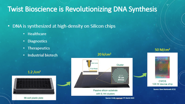
Twist Bioscience revolutionized DNA synthesis by transitioning from a traditional nanowell-plate-based process to a silicon-chip-based platform. Leveraging inkjet technology, they patterned silicon chips with anchoring sites for DNA growth, achieving an impressive density of 20,000 spots (of unique oligos) per square centimeter.
As Twist Bioscience ventured into the emerging market of DNA data storage, they partnered with imec to address a critical challenge: increasing the throughput of their system.
To make DNA-based digital information storage economically viable, the throughput needed to scale by more than three orders of magnitude. Together with imec, they developed a custom ASIC chip integrated with an exceptionally dense array of electrochemical cells, all controlled by the ASIC.
Through a close collaboration, imec and Twist Bioscience succeeded in solving the technical challenges in the design and development of the ASIC. One of these challenges was the etching of the platinum electrodes at very small dimensions. Imec developed a dedicated process, tackling these and other challenges and ensuring a high-throughput, manufacturable system.
Imec's IC-Link division managed the ASIC supply chain to source a custom ASIC wafer on which imec did the post-processing part in its cleanroom. Ultimately, this effort led to the successful encoding of 1 gigabyte of data in a single synthesis cycle.
Imec’s in-house innovations
Imec's ability to think outside the box and tackle complex challenges is a key strength for its partners, complemented by an extensive expertise in process technologies and specialized features. Imec uses these assets also for in-house innovations, serving as demonstrators or potential technologies for future industry transfer.
A common thread in these innovations is their scalable and highly reproducible nature – enabled by the semiconductor platform – and their ability to enhance the performance of biological processes, measurements, or interactions.
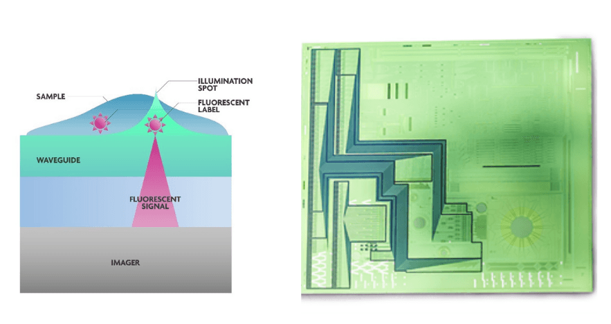
A prime example of such in-house innovation is the newly developed sub-pixel resolution lens-free fluorescence microscope-on-chip, which utilizes structured illumination.
The current sequencing landscape is dominated by two types of sequencers:
- CMOS-based sequencers that offer compactness but are limited in the number of reads per square centimeter
- lens-based sequencers, capable of achieving billions of reads per square centimeter, but with a large form factor
The novel concept developed by imec seeks to combine the best aspects of both approaches – delivering compact, high-throughput sequencing systems.
By integrating a fully functional optical stack – incorporating filters and waveguides – directly on top of an imager chip, imec made it possible to build highly miniaturized fluorescence microscopes-on-chip with large field of view and sub-pixel resolution. They are ideally suited for applications such as genome sequencing and proteomics, that benefit from parallel readout of large and dense molecular arrays.
A second example of imec’s in-house innovations is the work on solid-state nanopores.
Imec has developed a scalable process to mass-produce solid-state nanopores using deep UV lithography. This enables high-precision, low-variability nanopores, making them ideal for hybrid nanopore applications.
The mass producibility of these nanopores paves the way for innovations in personalized medicine, proteomics, and DNA memory, while also generating valuable data for optimizing nanopore performance.
Imec now offers a manufacturable nanopore platform and is seeking assay partners to further develop applications using its minimal viable demonstrator (MVD) – a multi-pore array with fluidics and read-out electronics.
Imec bridges the gap between flexible university fabs and high-end commercial foundries
For start-ups developing proof-of-concept technologies, the traditional commercial chip manufacturers are often inaccessible due to their high-volume requirements. Similarly, established companies may struggle to find a suitable foundry when they need highly advanced features or work with non-standard materials not supported by mainstream CMOS process flows.
University fabrication facilities present a flexible alternative, offering expertise in novel materials and advanced features. However, their infrastructure may not align with the latest commercial process flows, and their capacity for rapid prototyping and achieving a fast time-to-market is often limited by scheduling constraints and unreliable machine uptime.
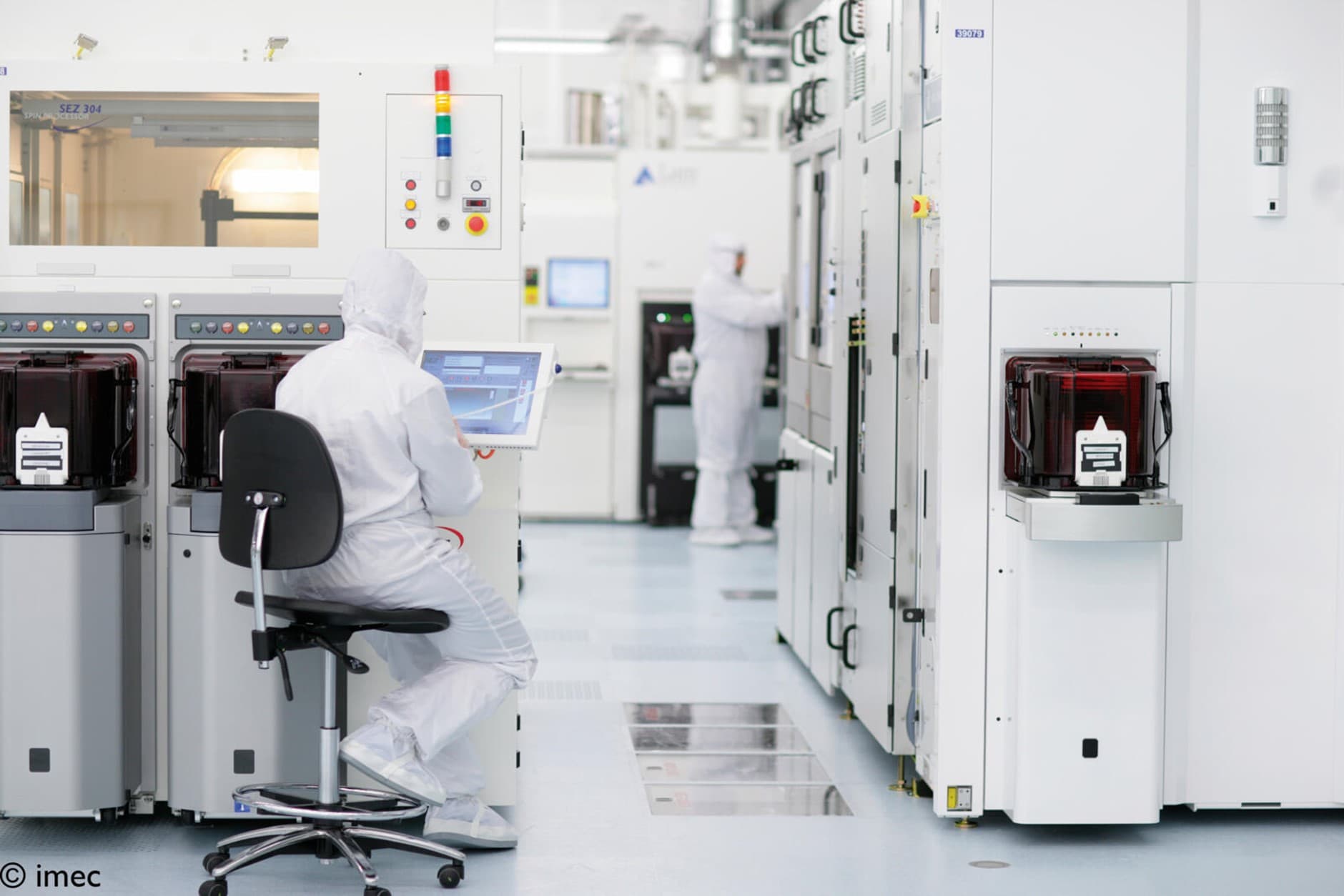
Imec addresses this gap by combining the flexibility and advanced capabilities of academic environments with the cutting-edge infrastructure and commercial expertise of a high-end foundry. Moreover, imec collaborates with an extensive partner network spanning the entire semiconductor ecosystem.
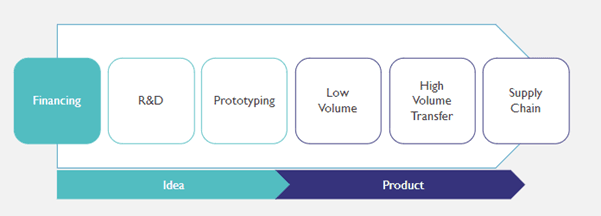
This allows biotech companies to benefit not only from prototyping and low-volume manufacturing but also from a seamless transition to large-scale commercial production at foundries through process technology transfer.
Beyond R&D: IC-Link enables custom chips for commercial products
Imec is widely recognized as a leading force in semiconductor R&D, collaborating with major industry players in large-scale ‘core CMOS’ research programs. Beyond this, imec – through its IC-Link division – has also set up a toolbox of platforms and services to enable custom chips on commercial-grade silicon, hereby connecting research to commercial products.
IC-Link is best known for its ASIC manufacturing and has now expanded its offering with new services and technologies which are particularly relevant for medical applications, where custom chips with non-standard materials and functionalities are often required – sometimes only in limited volumes. Such needs are not always easily met by large commercial foundries.
IC-Link’s toolbox includes:
- End-to-end ASIC manufacturing: flexible business models – ranging from full-turnkey solutions to custom-owned tooling – and adapted to diverse project needs. Global teams, with strong hubs in Europe and the US, provide in-house expertise across system architecture, project management, digital and analog design, and custom layout. Manufacturing is handled through leading foundries such as TSMC, with advanced packaging options including CoWoS. Imec also offers in-house test development and robust supply chain management, ensuring a seamless path from design to volume production.
- Integrated photonics: SOI-based wafer-scale integrated silicon photonics platform (iSiPP) and ultra-low-loss silicon nitride (ULLSiN), available on both 200mm and 300mm wafers. The platform includes a broad range of components such as waveguides, edge couplers, gratings modulators and detectors. The SiN variant is particularly suited for biotech and life sciences, supporting applications in visible-wavelength photonics.
- 3D integration services offering through-silicon vias (TSVs), hybrid bonding, flip-chip, heterogeneous integration via micro-transfer printing, and wafer reconstruction, enabling highly compact and efficient semiconductor designs.
- Access to manufacturing capabilities that do not have a standard flow, so-called specialty technologies, such as CMOS post-processing, lithography calibration wafers and the volume production of on-chip integration of imagers and detectors.
Specifically for medical applications, these process capabilities are of interest:- Advanced lithography: Dry 193 and immersion 193, e-beam, EUV and nanoimprint, for optical gratings and nanopores
- Post-processing of CMOS wafers: mirrors, band pass and lenses on imagers, active apertures on CMOS, low-temperature SiN photonics, nano-scale electrode material for biology applications
- Nano-optics: transparent substrates, high-refractive index materials for flat optics and high-index waveguides, microfluidics and glass processing: glass-to-silicon fusion bonding, integrated microfluidic components.
- Micro- and nanostructures: nanotips, nanochannels, nanopores, membranes.
The production of custom chips is mostly done at partner foundries, and in specific cases in the imec state-of-the-art 200mm and 300mm cleanrooms, but always through one point of contact: IC-Link. In this way, IC-Link can ensure a seamless transition to the required volumes, from multi-project wafers (MPW) to large-scale production via major partner foundries.
Want to know more?
- Read the white paper on monolithic microsystems to learn more about imec’s post-processing capabilities to build unique structures and specialty components on top of CMOS.
- Watch the recordings of the seminar ‘Disrupting bio with specialty silicon’, with imec experts from life science R&D, technology platforms, ASIC development, as well as from PacBio and Twist Bioscience.
- Discover IC-Link’s end-to-end ASIC offering and an example of collaboration with a health-tech company in this testimonial of Capri-Medical.
- Contact health@imec.be to discuss how imec can support your efforts in biotech.
Discover more