How imec contributes to massive single-molecule sensing arrays for proteomics
“It’s by combining different technologies into one integrated system that true innovation will be possible.”

This article is the third in a series of articles focusing on how semiconductor technologies can revolutionize proteomics.
We already gave an overview of the challenges and opportunities characterizing this domain and looked into how integrated sample prep can improve tools. In this article, we will dive deeper into the sensing part and how chip technology can contribute in making the tools and assays higher throughput, faster and more compact.
Want to stay informed about how semiconductor technologies revolutionize proteomics?
Click here to sign up for regular updates
To unleash the full power of proteomics – identifying and quantifying the full spectrum of proteins in a cell or tissue – new tools are arising.
Often, they rely on C-terminal immobilization of the proteins onto a solid surface, reading the N-terminal amino acid (using some sort of labels), and progressively degrading the protein (Edman-degradation-like techniques). Or on advanced-labeling techniques targeting specific sequences within the proteins.
In this article, we present some enabling components and technologies to move to more integrated, reliable and high-throughput proteomics solutions.
The proteomics landscape
The solutions in development and on the market today are incredibly innovative in the way they are tackling the main challenges in proteomics – the large dynamic range of protein concentrations & the fact that there is no easy way to amplify the proteins in a sample prep step.
The large dynamic range requires the analysis of billions of single molecules. This translates into large, ordered arrays of immobilization sites (e.g. electrodes or wells) in/on which a reaction takes place.
This reaction can be a degradation step (e.g. Edman degradation to ‘peel off’ one amino acid at a time) and/or an affinity-based binding step, identifying all or specific amino acids in the molecule. The affinity binder can be based on synthetic ‘recognizers’, DNA barcodes, fluorescent labels, etc. By reading these labels, feeding the data into a processing unit, and using machine learning and a reference database, the proteins can be identified and quantified.
The arrays can be manufactured using semiconductor processing techniques, related to the techniques employed for DNA sequencing.
“At imec, we are following these developments from close by, because we believe that we can contribute to this field just as we did with the 3rd generation of sequencing,” explains imec fellow Pol Van Dorpe.
“We have various disciplines and technologies in house: system design, modelling, characterization, biochemistry, (post-)processing, fabrication, etc. This makes it possible to fabricate micro- and nanostructures with patterned functionalization, and dedicated fluidics, (silicon nitride) photonics, and electronics. One of our strong assets is for sure our broad patterning capability ranging from EUV to nano-imprint lithography.
It’s by combining different technologies into one integrated system that true innovation will be possible.”
Silicon nitride photonics
Integrated photonic components guide and manipulate light on chip. The different material platforms that exist are mainly silicon-based. This allows to reuse the technology maturity and existing infrastructure of the CMOS fab, including the use of 300mm wafers, a high yield, co-integration with CMOS and 3D integration techniques.
Next to the silicon-on-insulator (SOI) or silicon platform – suitable for light with wavelengths in the 1 to 2 µm range – and the III/V material platform – enabling laser integration, there is a material platform that is especially interesting for life science (and proteomics) applications: silicon nitride photonics (SiN).
SiN exhibits lower light losses and a broader spectral coverage (including visible and near-infrared) than the more standard Si platform. Visible light wavelengths are typically used to excite the fluorescent labels in proteomics assays. Also, there is a low-temperature process option that can be used to post-process photonic components on top of CMOS.
These are the mature SiN photonics platforms that are available at imec:
- Ultra-low-loss SiN, based on low-pressure chemical vapor deposition (LPCVD) for ultra-low loss applications; available on 200mm wafers; wide wavelength range from 450nm to 2400nm; extremely low waveguide loss: < 0.1 dB/cm down to 2 dB/m.
- Low-temperature CMOS-compatible SiN, based on plasma-enhanced chemical vapor deposition (PECVD) for integrated photonics on top of CMOS imagers and flat optics; available on 200mm and 300mm wafers; wide wavelength range from 450nm to 2400nm; low waveguide loss: < 2 dB/cm down to 0.3 dB/cm
Next to this, imec also has SOI, co-integrated Si/SiN and III-V-on-Si(N) material platforms available. The uniqueness of imec’s expertise lies in the fact that different disciplines can be combined with the integrated photonics capabilities.

Patterned surface functionalization at wafer scale
Surface functionalization is closely linked to microfluidics and immobilization of molecules on solid surfaces. It involves modifying the surfaces to achieve specific properties or interactions with fluids and biomolecules. Examples are controlled wettability, prevention of biofouling, and selective binding and capture of specific molecules.
In its cleanroom, imec has a unique tool (NVD300 from KLA) to functionalize full batches of wafers with different chemistries at a time, and – combined with its lithography toolset – in a patterned way. This is a unique asset which enables cost-efficient fabrication of proteomics chips.
Nanoimprint lithography embedded in advanced lithography fab
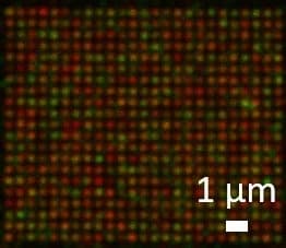
Proteomics often requires the analysis of large arrays of molecules. Nanoimprint lithography (NIL) allows for cost-effective patterning on top of different types of substrates (including glass substrates). This includes the patterning of physical structures (e.g. nanowells), and chemistry.
Imec is able to run NIL processes on both 200 and 300mm wafers, both for patterning of dielectrics, semiconductors and electrodes as well as for patterning surface chemistry. Moreover, imec has the established capability to produce master templates using its 300mm pilot line, with very small and high-density features.
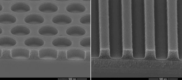
Next to the above-mentioned enabling technologies and tools, imec has developed interesting components over the years that illustrate its capabilities and can be relevant for proteomics tools.
Fluorescence microscopy-on-chip
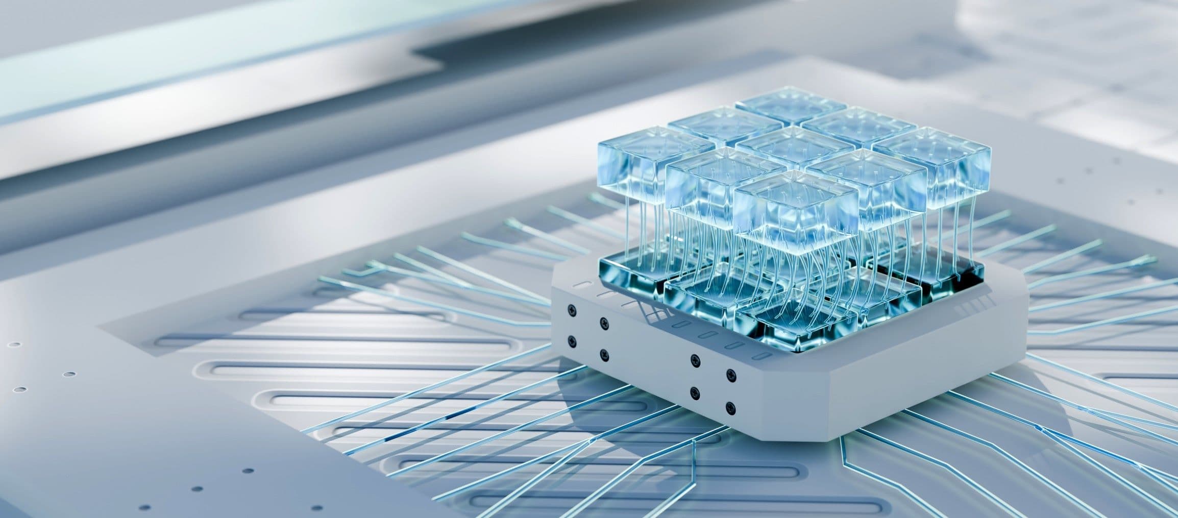
“A first valuable example showcasing the potential of chip-based processing is a chip-scale fluorescence microscope,” highlights Niels Verellen, scientific director and R&D team leader integrated biophotonics.
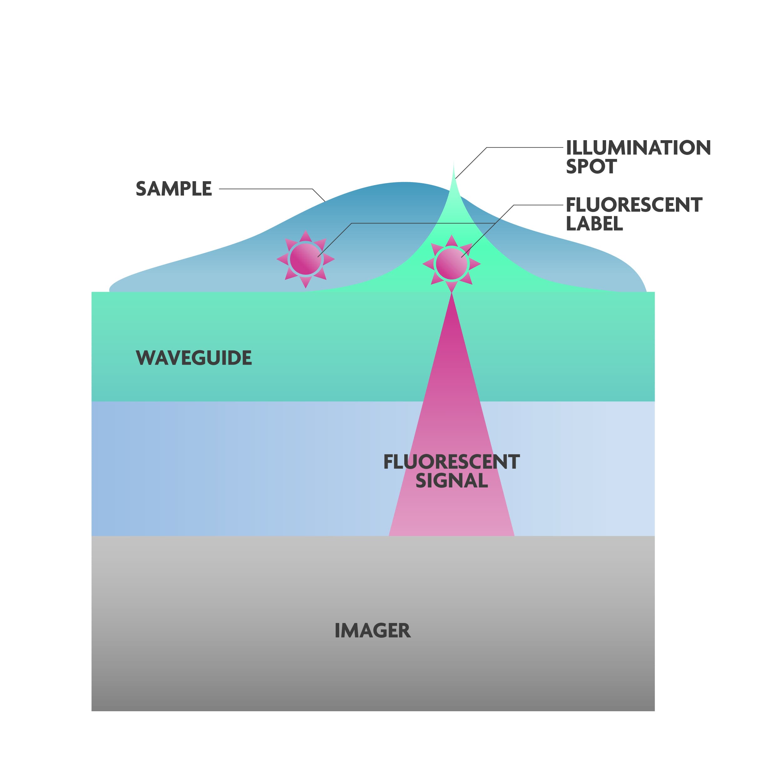
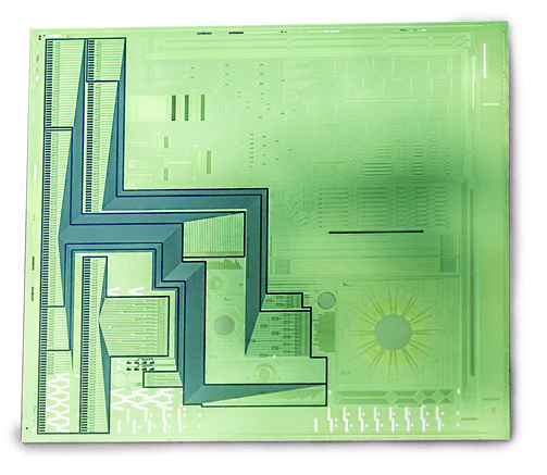
“It could turn today’s fluorescent-based proteomics solutions – utilizing external microscopes – into more high-throughput and user-friendly systems. It is a lens-free microscope that uses structured illumination to realize sub-pixel resolution. It enables parallel readout of large and dense molecular arrays like in proteomics applications.”
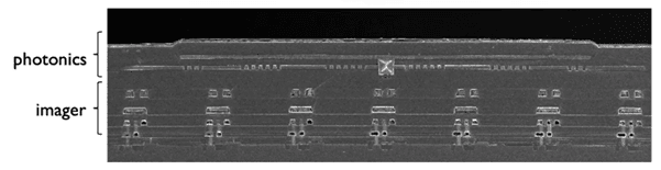
The microscope-on-chip uses integrated photonic components on top of imagers to illuminate the fluorescent-labelled proteins with the excitation wavelength:
- Waveguides guide the excitation light in the chip.
- Phase modulators shape the light into individual spots, a spot per molecule.
This ‘spot pattern’ is created by generating interference patterns based on the wave characteristics of the laser light. A spot of light appears in regions where the combined waves reinforce each other – constructive interference – while it remains dark in regions where the waves cancel each other out – destructive interference.
Niels Verellen adds: “A mathematical model was built to be able to generate the desired pattern of spots, and this in turn was translated into a unique chip architecture with photonic components on top of imagers, with a dedicated filter in between. The filter rejects the excitation light so that only the fluorescence emission reaches the imager.”
Bio-FinFETs for real-time immuno-assays
Charge-based sensors are an alternative to the more conventional optical approaches. It has the advantage that the biosensors can be directly integrated with the read-out circuitry, enabling faster processing.
Also, with billions of transistor-based sensors fitting onto a chip, unprecedented parallelization is possible, paving the way for high-throughput sensing platforms.
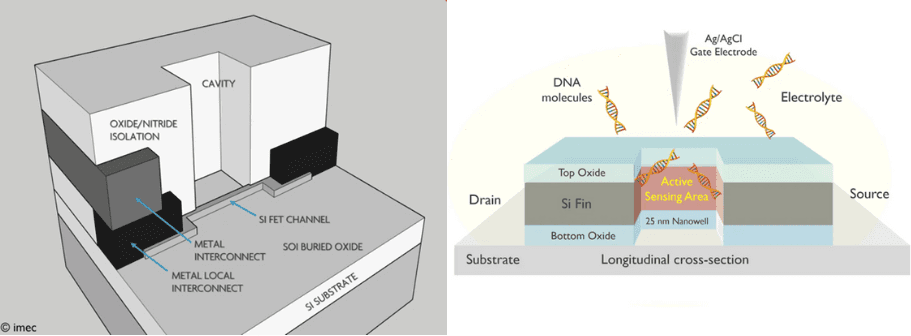
“Traditional transistors such as MOSFETs can be transformed into liquid-gated FETs which can act as a biosensor for DNA or proteins, to be fabricated and read out in large arrays,” explains Pol Van Dorpe.
“A change in threshold voltage can be measured when biomolecules attach to the functionalized dielectric surface. The challenge is to make very narrow ‘nanowire’ gates and to make this electronic component compatible with a liquid environment.
At imec, we succeeded in making the smallest silicon FinFET-based biosensor in this way – with a 50nm long channel. Moreover, building further on this concept, we realized a nanowell FET with a 25nm nanowell as the active sensing area in a 35nm-wide nanowire. The addition of the nanowell increases the sensitivity of the device.”
Photonic circuits for real-time immuno-assays
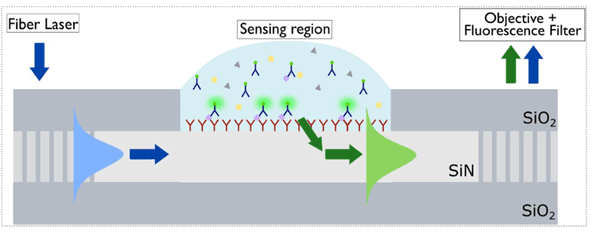
Imec developed a photonic-based device that can act as a real-time immuno-assay tool with high sensitivity and specificity.
Pol Van Dorpe describes the concept: “The device uses a laser source for the excitation light and a waveguide that guides the light to a functionalized sensing area. If the target molecules – with a fluorescent label attached – bind to the sensing area, the fluorescent light that is emitted travels further through the waveguide and can be detected via a filter – filtering out the background signal – and objective.
This results in sub-pM sensitivity and a high specificity. As this is based on chip technologies, a high level of parallelization is possible, leading to very fast and efficient assay results.”
Conclusion
Imec's multidisciplinary expertise across various domains, including system design, CMOS processing, biochemistry, fluidics, and photonics, is a valuable asset for proteomics innovation.
For example, leveraging integrated photonics technology, imec has developed chip-scale fluorescence microscopes capable of high-throughput protein analysis, eliminating the need for external microscopes and streamlining the process.
Additionally, imec's nanowell-FETs and dedicated photonic circuits offer real-time immuno-assay capabilities with unparalleled sensitivity and specificity. These novel biosensors enable rapid, efficient, and parallelized protein detection, paving the way for powerful tools to unlock the mysteries of the proteome and advance biomedical knowledge and therapies.
More reading
- Find more information on e.g. imec’s electrode and photonics expertise in our monolithic microsystems white paper.
- Read more on integrated photonics concepts for realtime immuno-assays in the technical paper ‘Suppression of bulk fluorescence noise by combining waveguide-based near-field excitation and collection’.
- Read more on the FET-based sensors in the invited ECS paper ‘BioFETs and Nanopore FETs: Nanoscale Silicon Field-Effect Transistors for Single-Molecule Sensing’.
- Find the details on the fluorescence microscope on chip.
- Explore more information on the mathematical model for the structured illumination in the lensfree fluorescence microscope in the technical article ‘Inverse design assisted coherent optical lattices’.
Authors

Pol Van Dorpe
Pol Van Dorpe received his PhD from the faculty of engineering of KU Leuven for his work in the field of spintronics. Afterwards he was appointed as a postdoctoral fellow of FWO-Flanders (2006-2012), based at imec, where he focused on metal-based nanophotonics and plasmonics for biosensors and energy-harvesting. During this period, Pol worked for some time at Stanford University, where he set up worldwide collaborations with renowned scientists in this field. His work has led to over 100 peer-reviewed papers in high-impact factor journals and has attracted more than 5000 citations. Since 2012 he has held the position of part-time associate professor in the physics department at KU Leuven and he is a leading member of staff in the life sciences department at imec, where his main research focus is applying integrated photonics concepts to enable novel applications in the life sciences field.

Niels Verellen
Niels Verellen is a senior photonics researcher and project leader at imec’s Life Science Technologies department, where he works on integrated photonics technologies for life science applications. As a research fellow, he is also affiliated to the KU Leuven Solid State Physics and Magnetism group. Niels received his Master (2007) and PhD (2011) degrees in Physics from KU Leuven. For his PhD research in the field of plasmonic nanomaterials, performed partly at imec, he was awarded the Umicore Scientific Award 2012 (€10,000). From 2011-2016, he was FWO postdoc at KU Leuven and imec, investigating light-matter interactions with optical nanoantennas and near-field imaging beyond the diffraction limit. In 2014, he worked on optical quantum sensing at the California Institute of Technology (Caltech) as visiting postdoctoral fellow. He (co--)authored close to 50 peer-reviewed publications which have been cited over 1800 times. Recently, he received the prestigious ERC Starting Grant for the development of a high-resolution on-chip fluorescence microscopy platform.
Discover more