The promise of hybrid graphene/metal structures for advanced interconnects
Hybrid structures of graphene and metal are worthy candidates for extending the back-end-of-line technology roadmap beyond 1nm.
This article takes a closer look at two of these hybrid schemes: a graphene-capped metal interconnect and a stack of alternating graphene/metal layers.
The authors discuss the potential of using these hybrid structures as advanced interconnects, they highlight the crucial role of (engineering) the interface between the two conducting materials and list the remaining integration challenges.
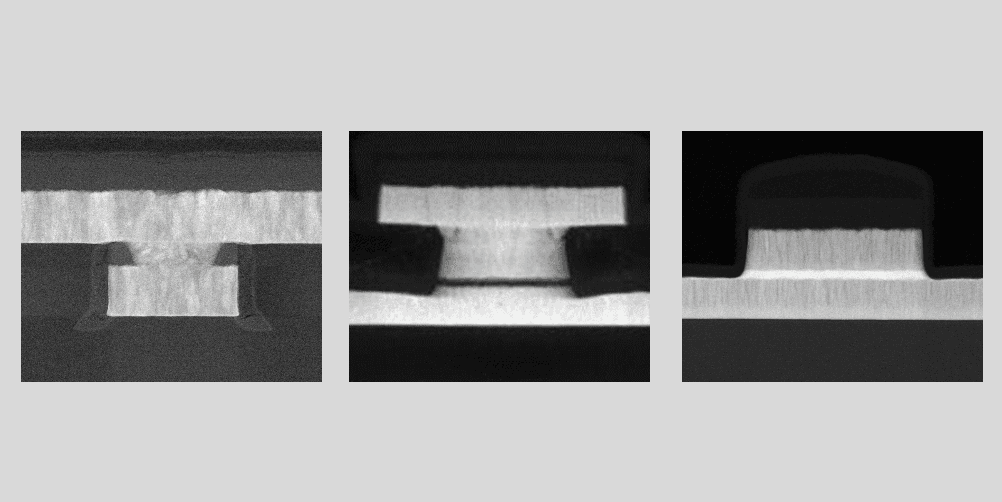
At the 2021 IEEE International Interconnect Technology Conference, imec presents other options for scaling the back-end-of-line.
Advancing the chip’s back-end-of-line
While chipmakers continue to make advancements with transistor technologies in the front-end-of-line (FEOL), the interconnects within the chip’s back-end-of-line (BEOL) are challenged to keep pace. This BEOL is organized in different metal layers (local, intermediate, semi-global and global) which are vertically interconnected by means of via structures – filled with metals. With each new technology generation, routing congestion and a dramatic signal delay (resulting from an increased resistance-capacitance (RC) product) become more and more problematic, forcing chipmakers to consider new integration schemes and materials for fabricating the interconnects.
For the 5nm technology node – the most advanced chip generation that has entered volume production – critical local interconnects have metal pitches as tight as 28nm. Cu-based dual damascene still is the workhorse process flow for making the interconnects. But with metal pitches soon moving towards 21nm and beyond, chipmakers may gradually move away from mainstream technologies. Imec, for example, foresees the introduction of alternative integration schemes such as hybrid via metallization, a semi-damascene process and hybrid height with zero via for the nodes to come.
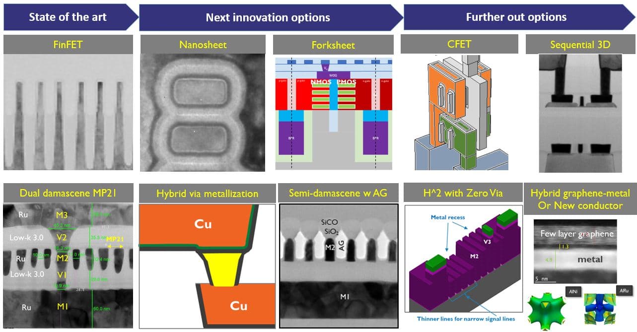
In parallel, alternative conductors with better figure of merit are being investigated to be used in combination with these advanced process schemes. This figure of merit is defined as the product of the bulk resistivity and the mean free path of the carriers in the metal. Of interest are cobalt (Co), ruthenium (Ru), tungsten (W) and ordered binary intermetallic compounds such as AlNi or RuV3.
In addition, researchers look intensely at graphene, which, thanks to its remarkable properties, is making its way into many interesting fields of application such as (bio)sensing, energy storage, photovoltaics, opto-electronics and CMOS scaling.
Why graphene?
In recent years, graphene has been intensively studied for interconnect applications, where it has potential to fulfill diverse roles. The material has for example been considered as an oxidation barrier and as an ultrathin diffusion barrier for metals. Researchers have also investigated the feasibility of using multilayer graphene wires or nanoribbons as an alternative conductor.
Interest in graphene for interconnect applications comes as no surprise. Graphene exhibits a high intrinsic carrier mobility (up to 200,000cm2V-1s-1) and a large current carrying capacity (up to 108A/cm2). In addition, graphene has a high thermal conductivity and competitive robustness against electromigration. It can also be made atomically thin, which helps alleviating the thickness contribution to the RC delay.
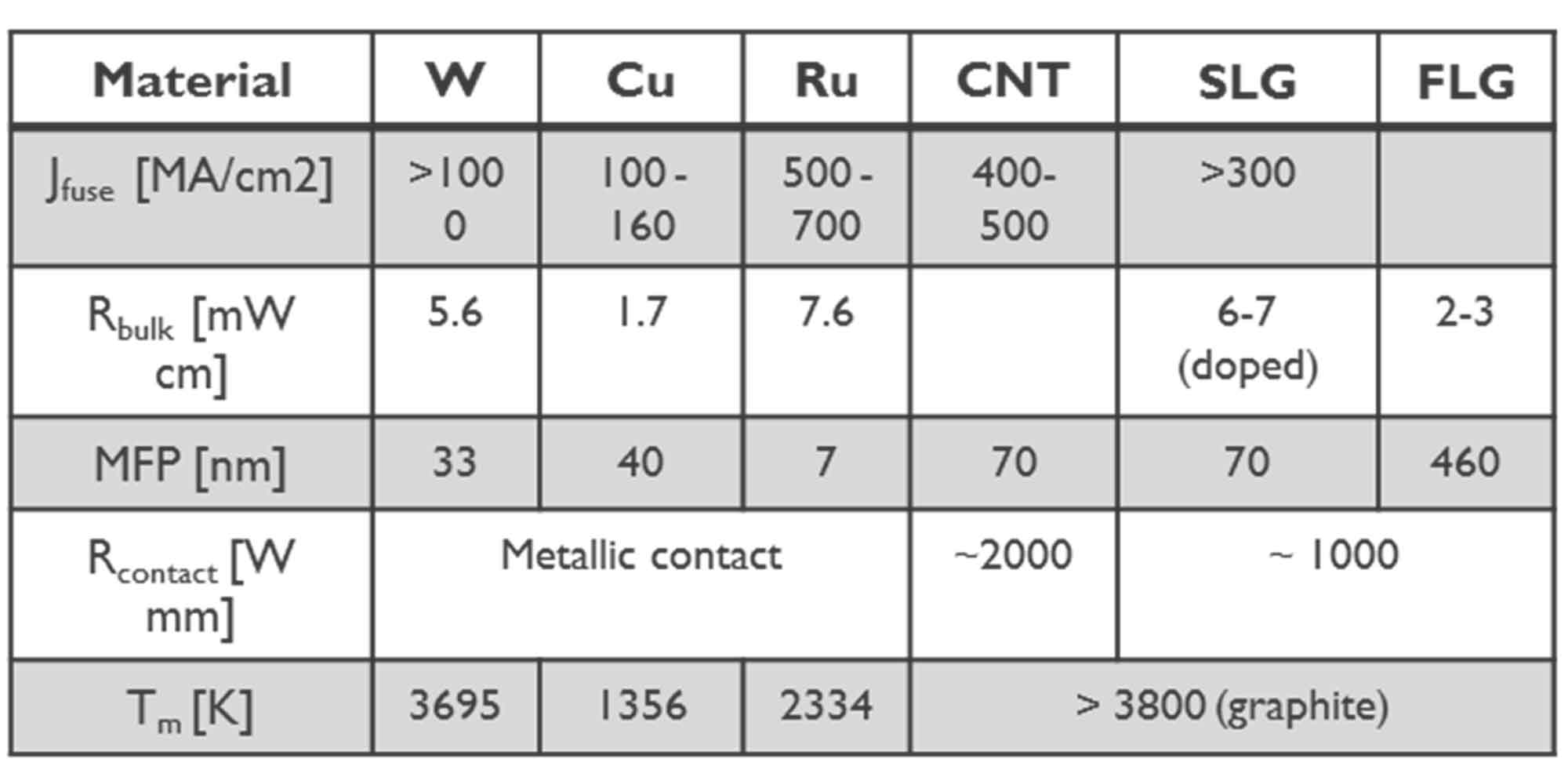
Despite these interesting properties, graphene has one major drawback: intrinsically, it does not hold enough charge carriers to be useful as a local interconnect. The lack of charge carriers severely reduces its electrical conductivity, a key metric for interconnect performance that is proportional to both the mobility and the carrier concentration. For this reason, several layers of graphene will be needed to cross-over Cu for example, for (local) interconnect applications – as confirmed by modelling. The number of layers will be a trade-off between the material’s overall contribution to resistance and capacitance.
Fortunately, there are ways to further modulate graphene’s conductivity. This has driven the research of so-called graphene nanoribbons – graphene layers patterned into narrow strips. The specific angular orientation of the graphene layers with respect to their underlying layer provides another knob for improvement. Finally, the conductivity of graphene can be boosted by doping, this way providing graphene with extra electrons or holes to carry the current. Doping can be performed in several ways, for example by metal-induced doping – enabled by bringing graphene in direct contact with metals like Cu or Ru. These hybrid metal/graphene schemes bring together the best of both ‘worlds’: the high carrier concentration of the metal and the high mobility of graphene.
This article looks into the feasibility of using hybrid metal/graphene structures for sub-2nm interconnect applications. Two different structures are being examined: graphene-capped metal and metal-capped graphene devices. The study focuses on Ru as a metal of interest, as it has recently emerged as a potential alternative for Cu metallization. But the concepts presented here are expected to be expandable towards other ‘interconnect’ metals.
Capping Ru with graphene
For this study, the imec researchers realized Ru/graphene hybrid structures by transferring a multilayer graphene film (grown by chemical vapor deposition (CVD)) onto a thin Ru film (typically 5nm) that was grown by physical vapor deposition (PVD). After transfer, graphene was found to adhere well to the large area PVD Ru film.
Of interest for interconnect applications is the metal-induced doping of graphene that is expected to happen at the interface with Ru. To understand and be able to control the doping, the charge transfer at the Ru/graphene interface was systematically investigated. The two main observations can be summarized as follows. First, the researchers found that the sheet resistance of Ru dropped by an average of 15% after encapsulation with graphene. Second, they observed a downward shift of graphene’s Fermi level into the valence band by ~0.5eV compared to intrinsic graphene, corresponding to a hole concentration of 1.9E13cm-2. This observation is an indication of metal-induced doping that happens at the interface, causing graphene to become p-doped when added as a capping layer to Ru.
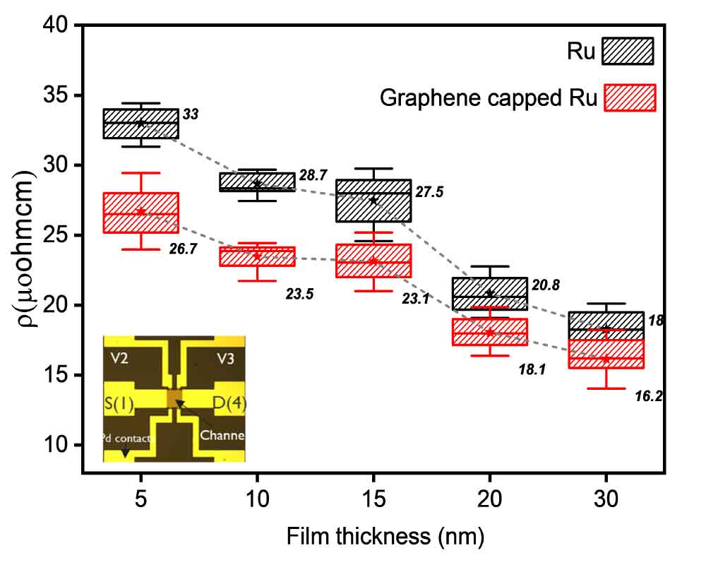
From this study, it has become clear that encapsulating Ru with graphene can boost the electrical performance of Ru as an interconnect. Yet, more fundamental insights are needed to determine the exact conduction mechanism taking place within the capped structure. Either Ru remains the main conductor, with graphene helping to reduce its resistivity by suppressing scattering mechanism(s) in the metal. Or the two conductors now act in parallel, with a higher conductivity for graphene (with respect to intrinsic graphene) because of the charge transfer. Modelling work is currently ongoing to get a better understanding.
It should also be noted that the Ru lines are observed to be less sensitive to temperature fluctuations when encapsulated with graphene. This could be due to the high thermal conductivity of graphene, providing an alternative/additional path for efficient heat dissipation. This observation is of interest for future interconnect applications, as the self-heating in highly scaled IC wires and an insufficient heat dissipation to the surrounding dielectric can degrade the interconnect’s thermal reliability.
Overall, the researchers conclude that these graphene-capped metal hybrid structures provide an answer to the RC delay problem for future interconnects. Imec envisions their introduction in the BEOL technology roadmap for the 1nm node and beyond.
A metal/graphene sandwich structure
In the longer term, researchers at imec are looking into stacking alternating layers of graphene and metal to further boost the electrical conductivity. In such a metal/graphene/metal/... sandwich-like structure, a second and different interface will now play an equally important role: the interface that results from depositing a layer of metal on top of graphene. Just like in the above study, the nature of the graphene/metal interaction at the interface can modify the physical properties of graphene. And its electronic band structure can also be significantly altered by the charge distribution at the interface.
Engineering the graphene/metal interface is however one of the most challenging bottlenecks. The (as-transferred) graphene layer typically contains many randomly oriented grains where the grain boundaries act as line defects and nucleation centers for metal deposition on top surface. This makes it challenging for depositing a metal uniformly covering the entire basal plane of graphene by means of traditional deposition method such as PVD or ALD. Moreover, after transfer, the graphene surface suffers from contamination – calling for a suitable cleaning method that does not damage the graphene layer.
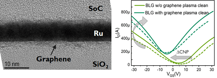
In a laboratory study, the imec researchers performed a hydrogen plasma cleaning of the graphene surface (by using an Ar/H2 downstream plasma), and subsequently deposited the metal (i.e., Ru) by using electron beam evaporation. It was then investigated how these processes affected the electrical conductivity of the graphene/Ru stack. They found that after exposure to hydrogen plasma, graphene experiences n-doping and a rise in charge carrier concentration. Unfortunately, single layer graphene also suffers from plasma-induced defectivity. Thicker graphene films are observed to be less affected. Under these conditions, an overall improvement of 18% in electrical conductivity of Ru-capped (plasma treated) graphene devices could be observed. These first results are encouraging, and further improvements can be expected by tuning the hydrogen plasma chemistry and conditions, and by increasing the number of alternating layers.
Towards industrial adoption...
These results demonstrate the performance potential of hybrid metal/graphene schemes in advanced interconnects. Yet, several integration challenges remain to be solved before these interconnect schemes can be adopted in a 300mm fab. For example, while this study focuses on graphene transfer, a more ‘elegant’ way of depositing graphene would be direct growth on the metal template of interest. Growing high-quality graphene requires however high growth temperatures (900-1000°C) and can as such not be applied on interconnect-type of metals. Deposition at lower temperatures has been demonstrated but comes at the expense of defectivity and reduced quality of graphene.
An alternative route which was applied in this study, includes the transfer of high-quality graphene – previously grown on platinum foils by using chemical vapor deposition (CVD). This transfer route provides an interesting approach when thermal budget is restricted. At imec, delamination and subsequent transfer of high-quality graphene on 300mm wafers has been demonstrated but might be challenged by the topography of the underlying metal layer. This process also comes with a significant addition of process steps and calls for improved uniformity and process control.
In addition, further research will be needed to optimally control the defectivity and specific orientation of the graphene layers. Studies at imec are ongoing to solve these integration issues and to turn the hybrid graphene/metal schemes into true industry-grade options.
Conclusion
Hybrid structures of graphene and metal are interesting candidates to extend the back-end-of-line technology roadmap beyond the 1nm technology generation. In this study, two options – graphene-capped metal and stacks of graphene/metal layers – have been discussed in more detail. In both cases, the interfaces between graphene and metal play a crucial role in the overall electrical behavior of the hybrid interconnect. While graphene-capped metal interconnects are the most mature, stacks of alternating layers may come into play in the longer term.
This article was originally published in Electronics Today, June 2021 edition.
Want to know more?
More details on these studies can be found in the following papers. Interesting in receiving these papers? Fill in our contact form.
- ‘Graphene-ruthenium hybrid interconnects’, S. Achra et al., presented at the 2019 IEEE International Interconnect Technology Conference (IITC).
- ‘Characterization of interface interactions between graphene and ruthenium’, S. Achra et al., presented at 2020 IITC. For this paper, Swati Achra received the Best Student Paper Award.
- ‘Enhancing interface doping in graphene-metal hybrid devices using H2 plasma clean’, S. Achra et al, Applied Surface Science 538 (2021) 148046.
- ‘Alternative metals: from ab initio screening to calibrated narrow line models’ C. Adelmann et al. Proc. IEEE IITC 2018.
Further reading on imec’s FEOL and BEOL roadmap:
- ‘A view on the logic technology roadmap’, imec reading room
More info on 2021 IITC can be found on the conference website.
Authors

Swati Achra
Swati Achra is pursuing PhD in Materials Engineering in MTM department, KU Leuven and at imec. She joined Nano-interconnects team at imec in 2017 and works on developing graphene enabled hybrid interconnects for future technology nodes. She received a joint MSc degree in Erasmus Mundus Masters in Nanoscience and Nanotechnology magna cum laude from KU Leuven, Belgium and Université Grenoble Alpes, France in 2017. During her master's thesis, she worked in Institut Néel, CNRS, France studying in-situ thermal transport in suspended graphene and CNT membranes. She received the L’Initiative D’Excellence (IDEX) Scholarship for European Graduate Programs. Prior to this, she was working as research intern in 2D materials team at imec for developing spin-on-dielectric assisted transfer of 2D TMDCs. She graduated B.Tech in Chemical Engineering and Materials Science with university gold medal in 2015 from Amrita Vishwa Vidyapeetham, Tamil Nadu, India.

Inge Asselberghs
Inge Asselberghs is program manager for exploratory logic at imec. She received the M.Sc. and Ph.D. degrees in chemistry from the University of Leuven, Leuven, Belgium, in 1998 and 2003, respectively. After a Post-Doctoral Fellowship in nonlinear optics, she moved to imec, Leuven, as a Researcher, where she was involved in exploratory 2-D-material-based device fabrication and characterization.

Zsolt Tokei
Zsolt Tokei is Distinguished Member of Technical Staff Interconnects at imec. He joined imec in 1999 and since then held various technical positions in the organization. First as a process engineer and researcher in the field of copper low-k interconnects, then he headed the metal section. Later he became principal scientist, Program Director Nano-Interconnects and, in 2016, was appointed Distinguished Member of Technical Staff Interconnect. He earned a M.S. (1994) in physics from the University Kossuth in Debrecen, Hungary. In the framework of a co-directed thesis between the Hungarian University Kossuth and the French University Aix Marseille-III, he obtained his PhD (1997) in physics and materials science. From 1998 he worked at the Max-Planck Institute of Düsseldorf, Germany, as a post-doctorate researcher. From the date of joining imec he continued working on a range of interconnect issues including scaling, metallization, electrical characterization, module integration, reliability and system aspects.
Discover more

A double world-first: integrating lithium niobate and lithium tantalate modulators on silicon photonics through micro-transfer printing
Read more
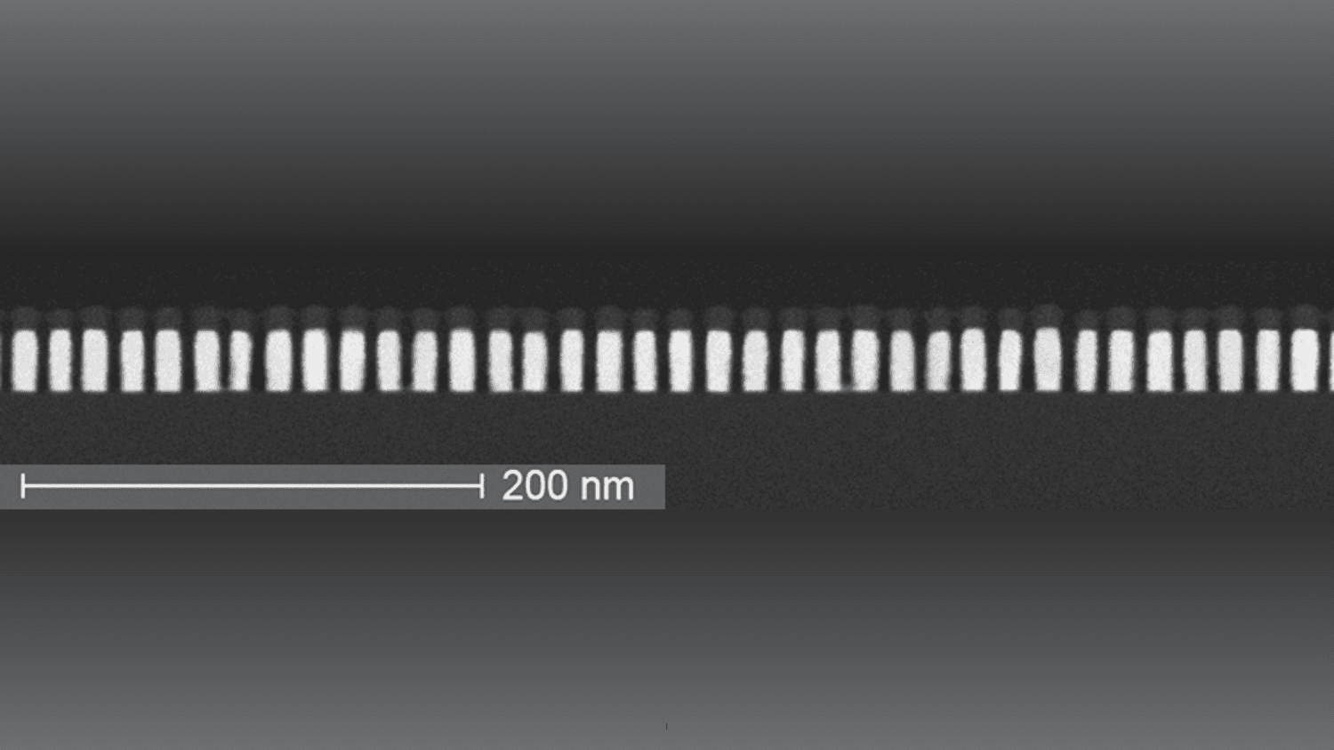
Imec demonstrates 16nm pitch Ru lines with record-low resistance obtained using a semi-damascene integration approach
Read more