Physical qubits for quantum computing
Imec leverages cutting-edge fabrication and state-of-the-art 300mm tooling for advanced semiconductor technology nodes to fabricate qubits at scale with high coherence times, low variability, and high yield.
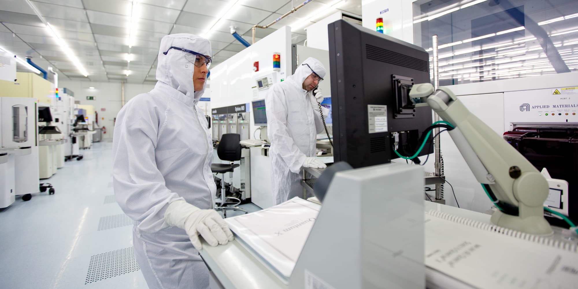
A large part of imec’s activities is devoted to the study of materials, as well as improving the quality of surfaces and interfaces in quantum devices. We utilize advanced test and characterization facilities to study the behavior of a range of materials and processes to identify the most promising options for qubit development.
Spin qubits
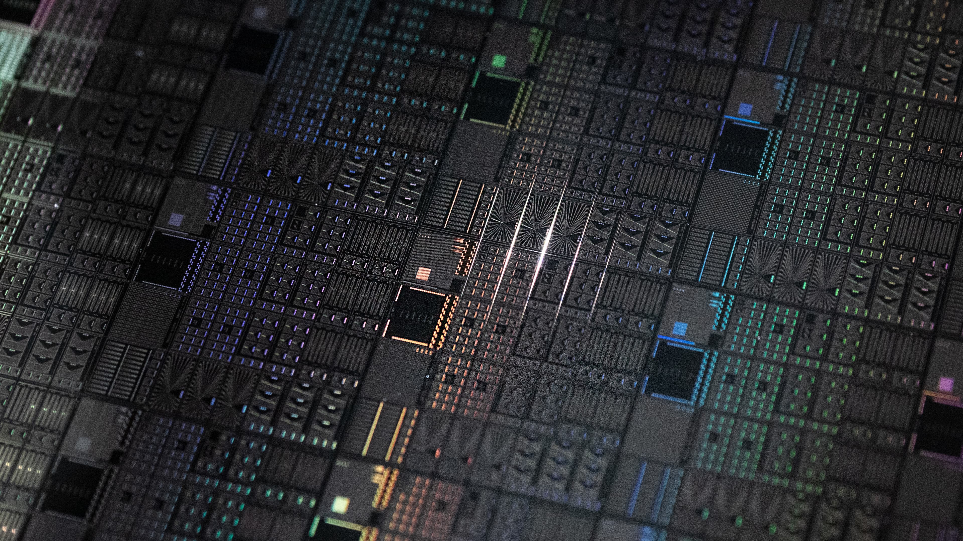
Spin qubit devices highly resemble standard CMOS transistors. We fabricate them on imec’s 300mm industrial fabrication line. The primary goal is to achieve:
- high quantum coherence and low qubit variability
- flexible back-end-of-line integration and control periphery for large-scale qubit arrays
In addition, standard CMOS characterization is coupled with cryogenic device testing towards understanding material properties and improving the process flow. This enables the accurate identification of those factors that limit the performance of qubits in relation to the fabrication process.
2026 press release: Imec presents quantum dot qubit device using High NA EUV lithography
2026 press release: Semiconductor-based quantum pilot line ‘SPINS’ launched with EU support
2026 article: Si MOS quantum dot spin qubits: roads to upscaling
2025 press release: Imec technology lights the path to utility scale for Diraq’s quantum chips
Superconducting qubits
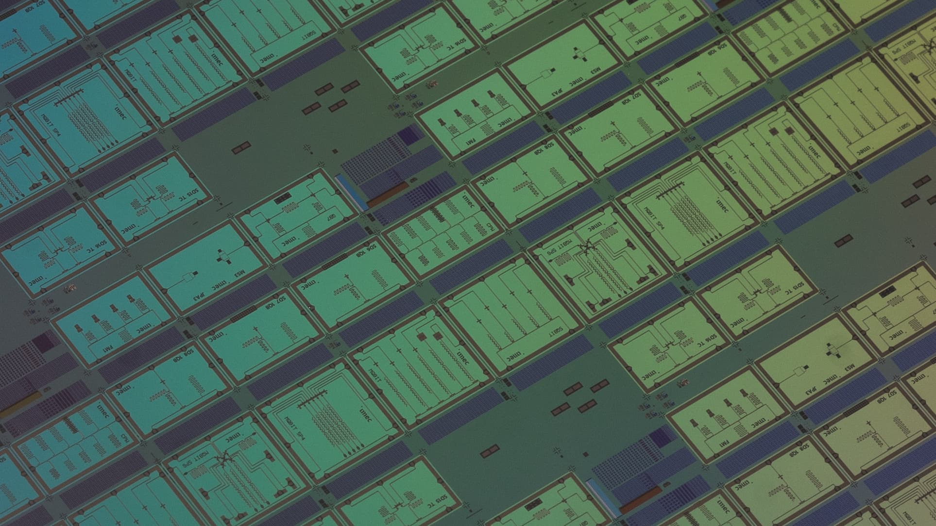
There’s a need for superconducting qubit fabrication techniques that can be fully integrated and are compatible with state-of-the-art 300mm industrial processing, including 3D integration.
Imec’s focus is on achieving high-coherence, low-variability, and high-yield quantum devices. To achieve these goals, we’re fabricating qubits and conducting extensive studies on materials, surfaces, and interfaces. New fabrication techniques are also explored, to ensure high-quality surfaces and interfaces. Those are critical to achieving high-fidelity superconducting qubits.
Cryo 3D integration
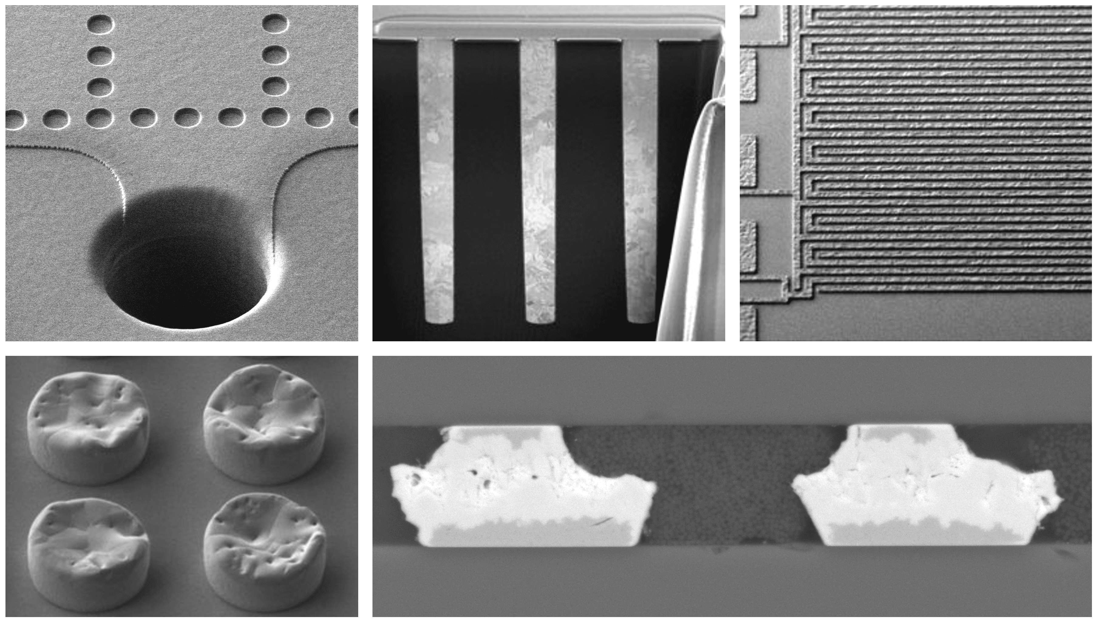
Imec's deep expertise in 3D integration on foundry-compatible 300mm platforms can be leveraged for quantum computing. Going to the third dimension can increase the density of qubits while reducing the footprint. It can also help address some of the scalability challenges currently facing qubit development.
With imec's 3D integration capabilities, it may be possible to interface large-scale qubit arrays with a standard industrial fabrication-compatible process.
Cryo CMOS device testing, and modeling
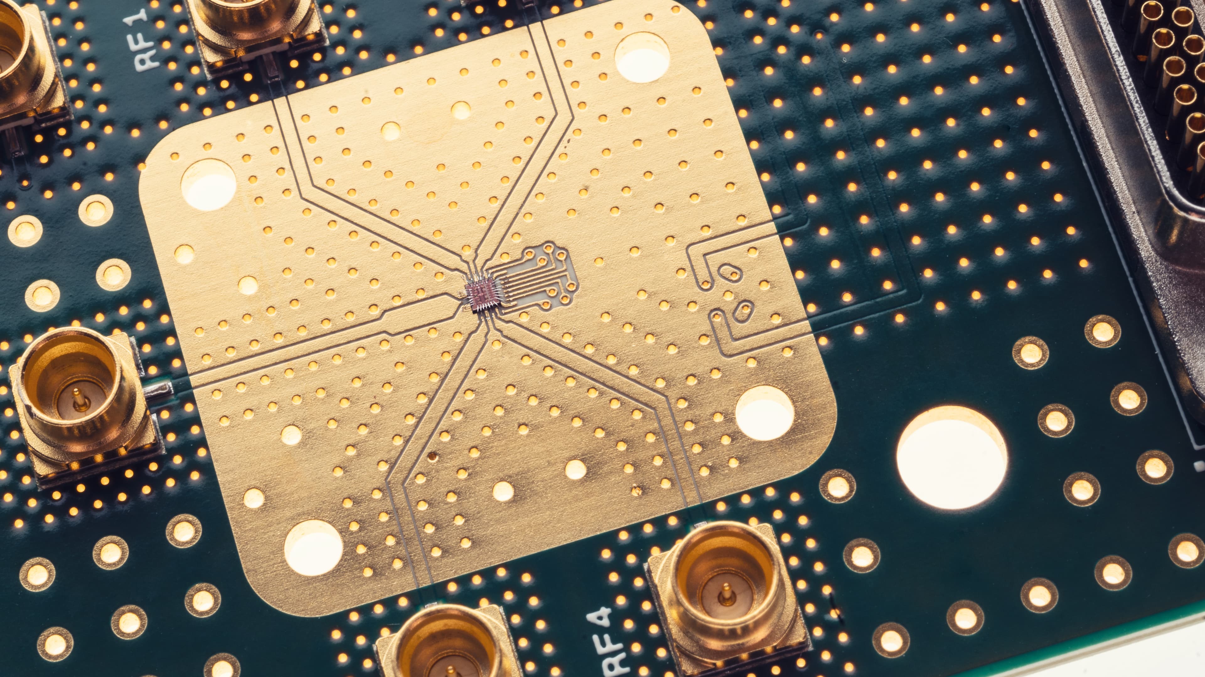
The complexity of future quantum computers could be tamed by dedicated classical supporting electronics. To enable scaling, reduce footprint, and minimize power consumption we’re exploring the behavior of classical CMOS electronics at temperatures down to the millikelvin regime.
We’re performing technology characterization and developing transistor models at cryogenic temperatures. Based on these foundations, we explore novel circuit concepts that can control qubits without degrading their performance.
Work with us
Want to accelerate your own quantum computing activities?
Through a bilateral R&D collaboration, you can leverage imec’s infrastructure and expertise. We offer support with both quantum devices and the periphery.
Imec not only helps you to address technological challenges. Thanks to our thorough knowledge of the industry, we function as your full-fledged strategic partner – right down to venturing support.
Scientific publications
Qubits
J. Verjauw et al. "Path toward manufacturable superconducting qubits with relaxation times exceeding 0.1 ms", npj quantum information, (2022)
External linkN. I. Dumoulin Stuyck et al. "Uniform Spin Qubit Devices with Tunable Coupling in an All-Silicon 300 mm Integrated Process", 2021 Symposium on VLSI Circuits, (2021)
External linkR. Li et al. "A flexible 300 mm integrated Si MOS platform for electron- and hole-spin qubits exploration", 2020 IEEE International Electron Devices Meeting (IEDM), (2020)
External linkMaterials
M. Mongillo et al. "High-Performance 300mm Integrated Superconducting Resonators for Quantum Computing Applications", 2021 IEEE International Electron Devices Meeting (IEDM), (2021)
External linkJ. Verjauw et al. "Investigation of Microwave Loss Induced by Oxide Regrowth in High-Q Niobium Resonators", Physical Review Applied, (2021)
External linkT N Camenzind et al. "High mobility SiMOSFETs fabricated in a full 300 mm CMOS process", Materials for Quantum Technology, (2021)
External linkCryo CMOS
R. Acharya et al. "Scalable 1.4 μW cryo-CMOS SP4T multiplexer operating at 10 mK for high-fidelity superconducting qubit measurements", IEEE Symposium on VLSI Technology and Circuits (VLSI Technology and Circuits), (2022)
External linkR. Asanovski et al. "New insights on the excess 1/f noise at cryogenic temperatures in 28 nm CMOS and Ge MOSFETs for quantum computing applications", 2022 International Electron Devices Meeting (IEDM), (2022)
External linkK.-H. Kao et al. "Linking Room- and Low-Temperature Electrical Performance of MOS Gate Stacks for Cryogenic Applications", IEEE Electron Device Letters, (2022)
External linkModeling and simulation
F.A. Mohiyaddin et al. "Large-Scale 2D Spin-Based Quantum Processor with a Bi-Linear Architecture", 2021 IEEE International Electron Devices Meeting (IEDM), (2021)
External linkF. A. Mohiyaddin et al. "Multiphysics Simulation & Design of Silicon Quantum Dot Qubit Devices", 2019 IEEE International Electron Devices Meeting (IEDM), (2019)
External linkG. Simion et al. "A Scalable One Dimensional Silicon Qubit Array with Nanomagnets", 2020 IEEE International Electron Devices Meeting (IEDM), (2020)
External linkNews and views
Phys.Org article: High-quality superconducting qubits fabricated with CMOS-compatible technologies
External linkEETimes article: Imec Demos Next-Level Superconducting Qubits
External linkImec press release: Imec Tenure-Track Holder Christian Haffner Awarded With ERC Starting Grant
Internal linkIEEE Spectrum article: Three Frosty Innovations for Better Quantum Computers
External linkImec press release: Xanadu and imec partner to develop photonic chips for fault tolerant quantum computing
Internal linkImec press release: imec and NUS to collaborate on chip-based quantum cryptography technology
Internal linkEU and national projects with active imec engagement
Other quantum activities
Read more
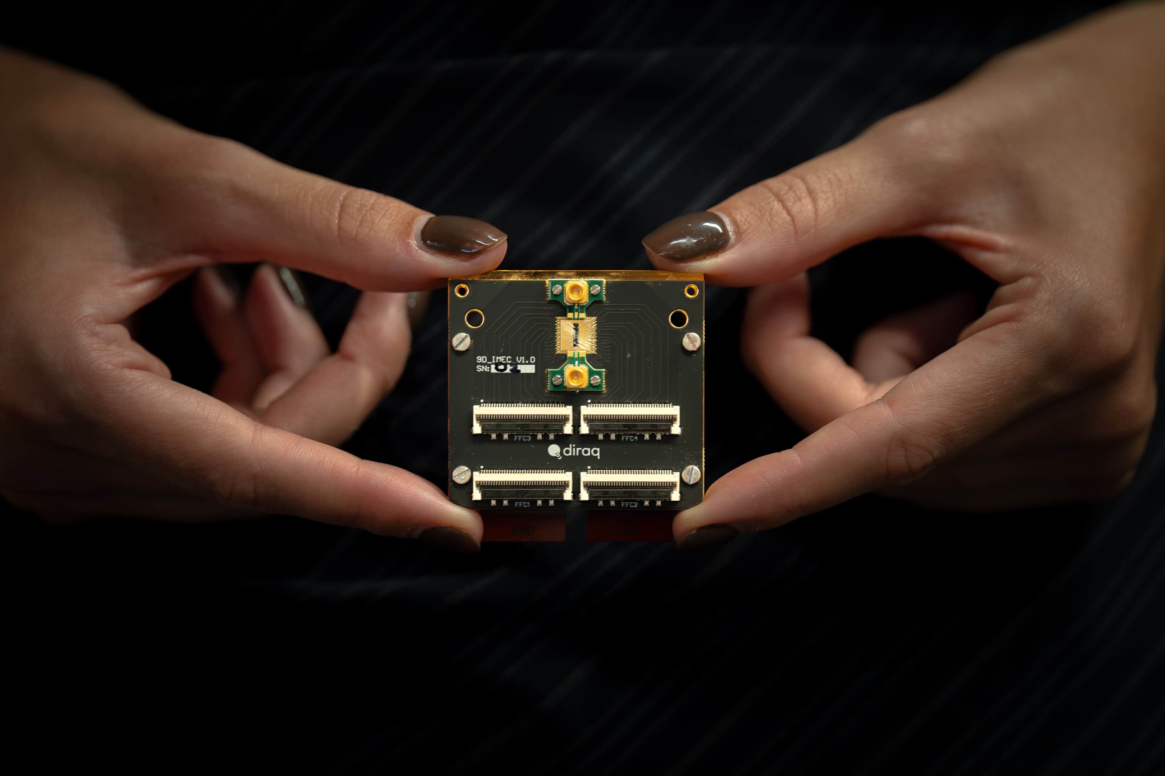
Imec and Diraq demonstrate first coherent operation of eight silicon MOS spin qubits fabricated in a 300mm CMOS-compatible foundry process
Result shows that industrial semiconductor manufacturing can support the scaling of silicon quantum processors beyond the two-qubit regime.
Read more
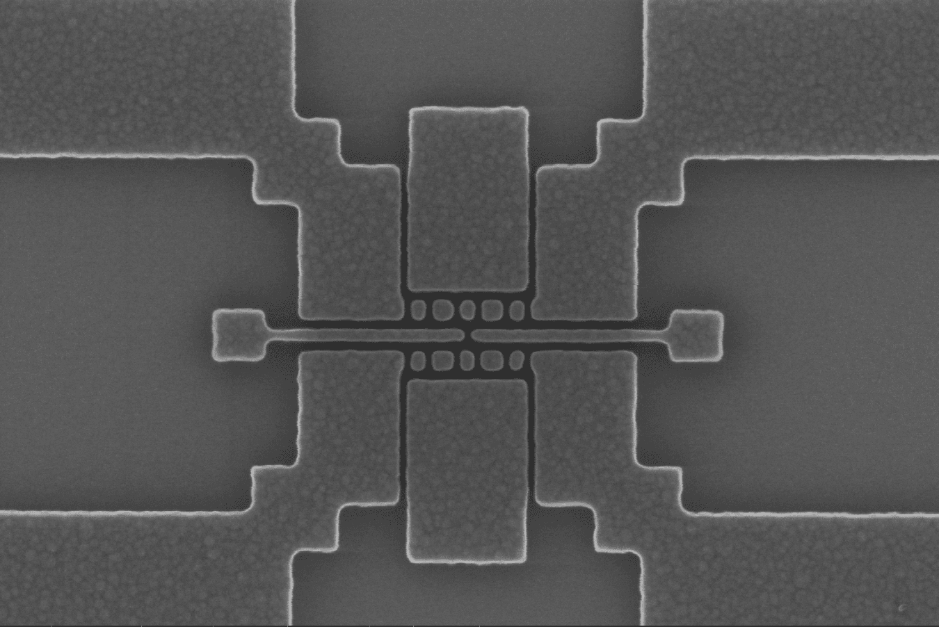
World first: imec presents quantum dot qubit device using High NA EUV lithography
The most advanced lithography system, crucial for future advanced memory and computer chips, will play a key role in scaling up quantum technology
Read more
ITF USA 2026 at SEMICON® West
From silicon to systems: building the AI future The pace of AI evolution leaves little room for certainty. Yet, several trends are clear: AI agents increasingly collaborating in orchestrated ecosystems are on the rise. Physical AI is a crucial next step, including (humanoid) robots transforming our homes and workspaces. In parallel, AI – just like advances in quantum computing – could help unlock breakthroughs in fields such as physics and biology. Building the AI future starts with a solid hardware foundation – from high-performance, energy-efficient compute in the data centers to low-power, real-time inference at the edge. ITF USA at SEMICON® West presents the building blocks for shaping the AI future. On October 12 in San Francisco, we take stock of the full AI deep-tech stack: from silicon to systems, from research to manufacturing. Discover ITF USA
View event