Semiconductor-based quantum pilot line ‘SPINS’ launched with EU support

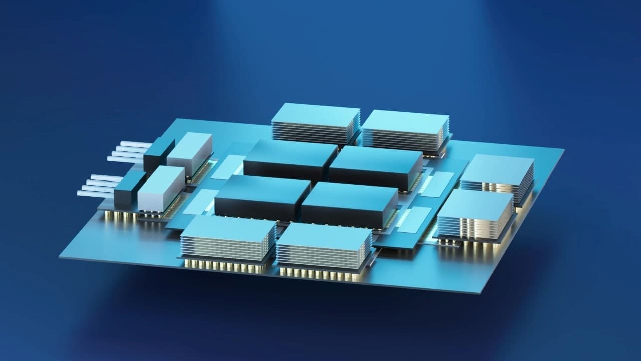
Leuven (Belgium), April 3, 2026–Today, ‘SPINS’ (Semiconductor Pilot line for Industrial Quantum NanoSystems) was launched, one of the 6 European quantum pilot lines. Coordinated by imec, the consortium brings together 25 European RTOs, industry partners, and academic research groups to strengthen Europe’s leadership and sovereignty in this strategically important domain. The €50 million SPINS pilot line project has been made possible through the co‑funding support from the European Union’s Chips Joint Undertaking (Chips JU) and the national and regional authorities of the participating Member States.
Quantum computing has become a highly strategic domain with economic and societal relevance rising sharply. Applications vary from breakthroughs in drug discovery and materials science to ultra-secure communications and next-generation navigation systems.
However, a gap remains between current quantum research and manufacturable quantum processors to enable significant quantum applications. Scaling the number of stable qubits (to as much as one billion) is key to building reliable and fault-tolerant quantum computers.
Given the technological complexity, including cryogenic operation, ultraprecise control electronics and highly specialized fabrication processes, and given the strategic importance of quantum chips, the EU Chips Act has established six complementary quantum pilot lines, each focused on a distinct hardware platform and collectively advancing quantum technologies in the space of quantum computing, communications and sensing.
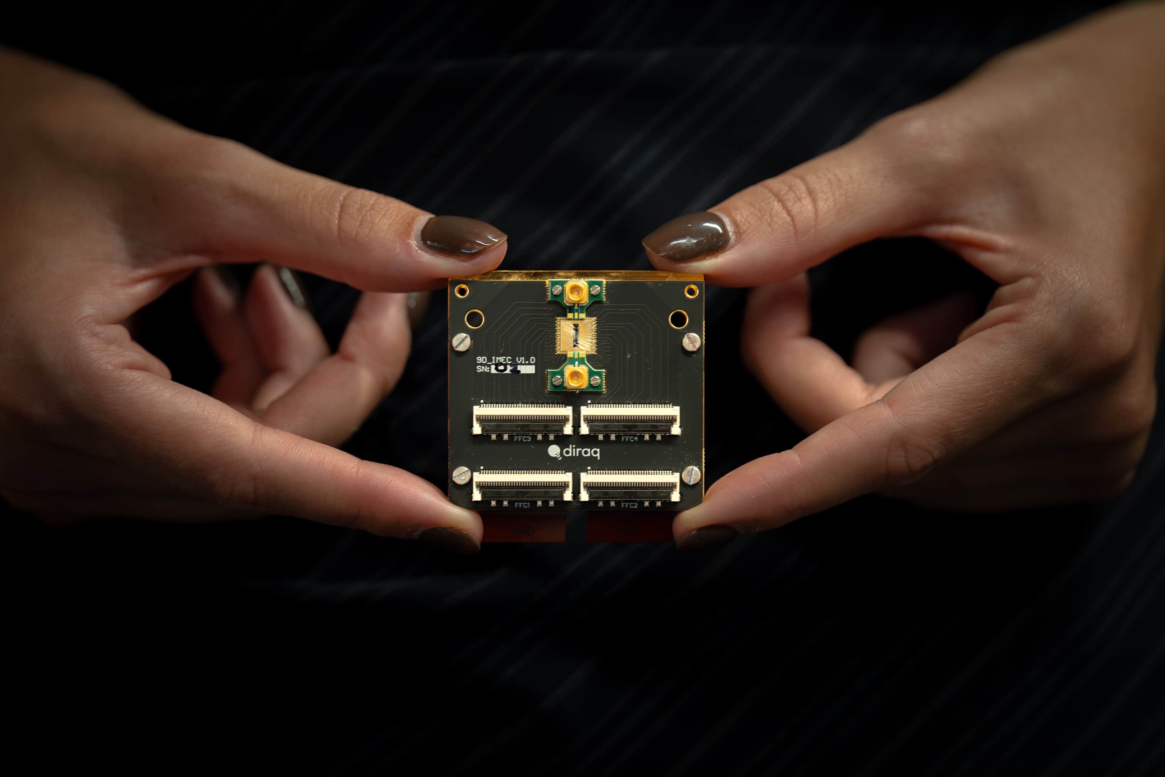
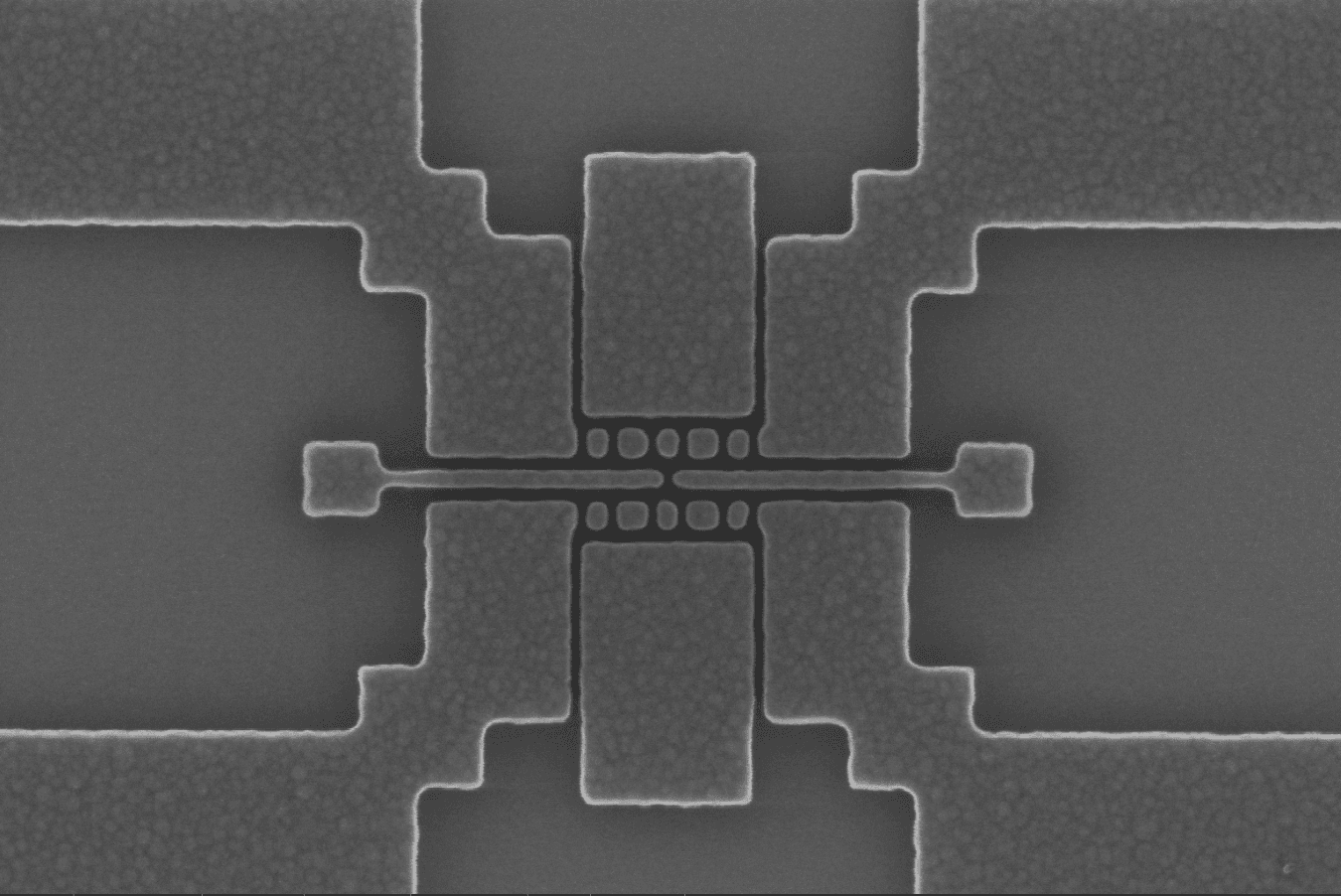
Within this portfolio, SPINS is the pilot line dedicated to semiconductor‑based spin qubits, with a primary focus on delivering quantum chips for quantum‑computing applications.
Imec coordinates this new pilot line efforts and leads the European consortium of 25 partners, ranging from RTOs like Fraunhofer, VTT and CEA-Leti, industry (both large enterprises like Infineon and Siltronic as well as SMEs and startups) and academic groups (like TU Delft and University of Jyväskylä), bringing in complementary knowledge and skills, with the goal of translating the strategic framework of the EU Chips Act into concrete actions.
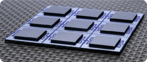
The first actions of the SPINS-consortium include process and design optimization to establish a robust foundation for scalable, stable, and high-performing spin qubits, all on three different technology platforms: Si/SiGe, Ge/GeSi, and SOI. SPINS aims to establish a lab-to-fab route for this technology via multi-project wafers (MPW) and standardized quantum process design kits (PDKs), which lower entry barriers for startups and SMEs in semiconducting quantum technology and lay the foundations for European companies to build quantum know-how early on.
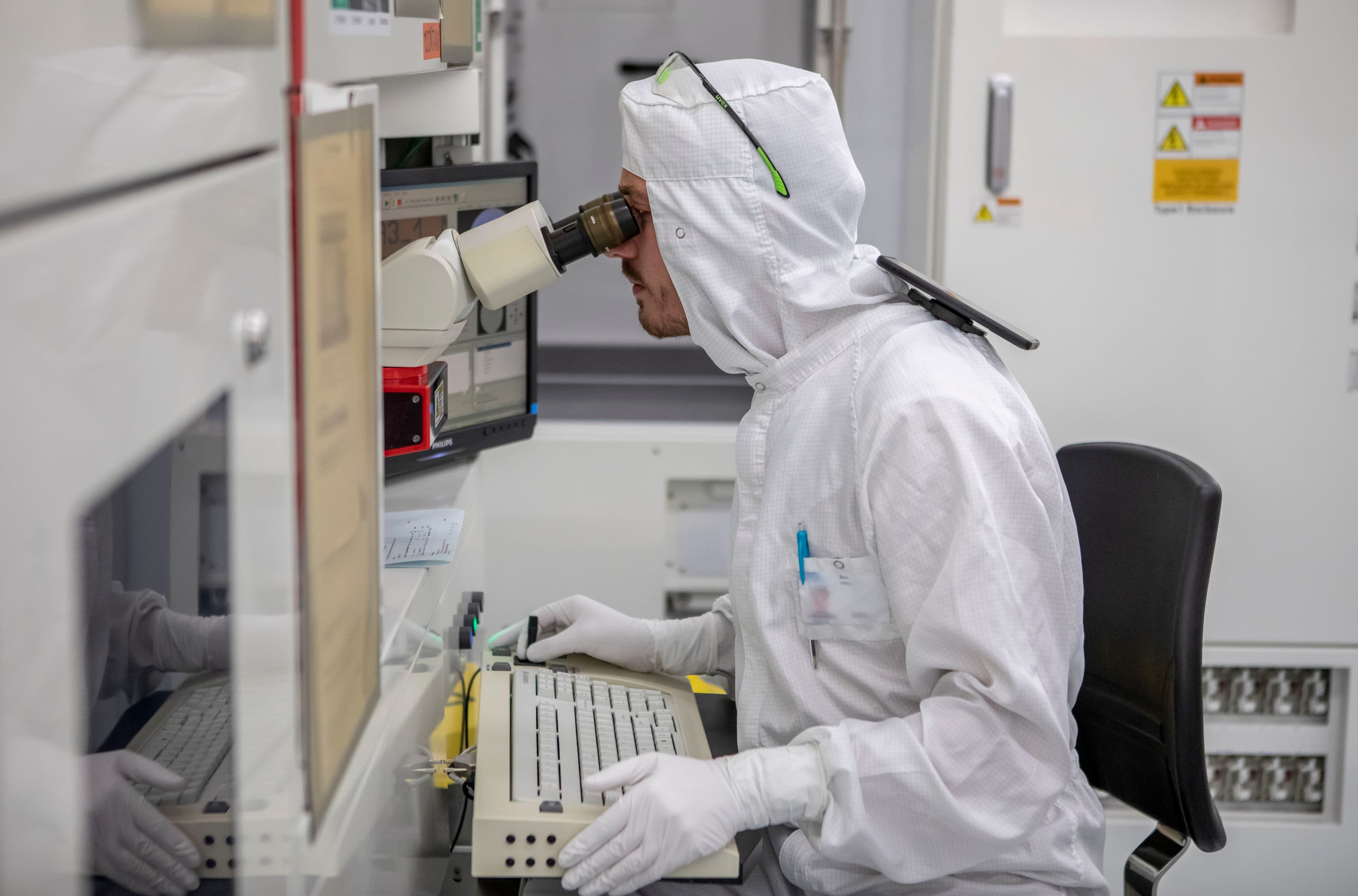
Kristiaan De Greve, coordinator SPINS: “Scaling qubits requires an extremely controllable environment and solid manufacturing processing, in view of the extreme sensitivity of qubits to environmental noise. These challenges require both the accuracy and control that is only present in state-of-the-art semiconductor cleanroom infrastructure, combined with the research and innovation mentality to adjust such an environment to address these sensitive qubits. At imec, we’ve been creatively addressing complex problems with advanced semiconductor manufacturing for over 40 years. By bundling the expertise of our European consortium partners in this quantum pilot line, we will speed up the development of high-TRL semiconductor qubits and thereby enable larger-scale quantum systems made in Europe.”
Complementary tracks of the European quantum efforts, next to the semiconductor-based pilot line, include pilot lines on photonics for quantum ‘P4Q’ (coordinated by University of Twente, NL) - to which imec is also contributing, ion trap qubits ‘CHAMP-ION’ (coordinated by SAL, AT), superconducting qubits ‘SUPREME’ (coordinated by VTT, FI), diamond quantum chips ‘DIREQT’ (coordinated by CNR, IT) and neutral atoms ‘Q PLANET’ (coordinated by Pasqal, FR).
About the European consortium partners
From Belgium
Imec, research and innovation center for nanoelectronics and digital technology.
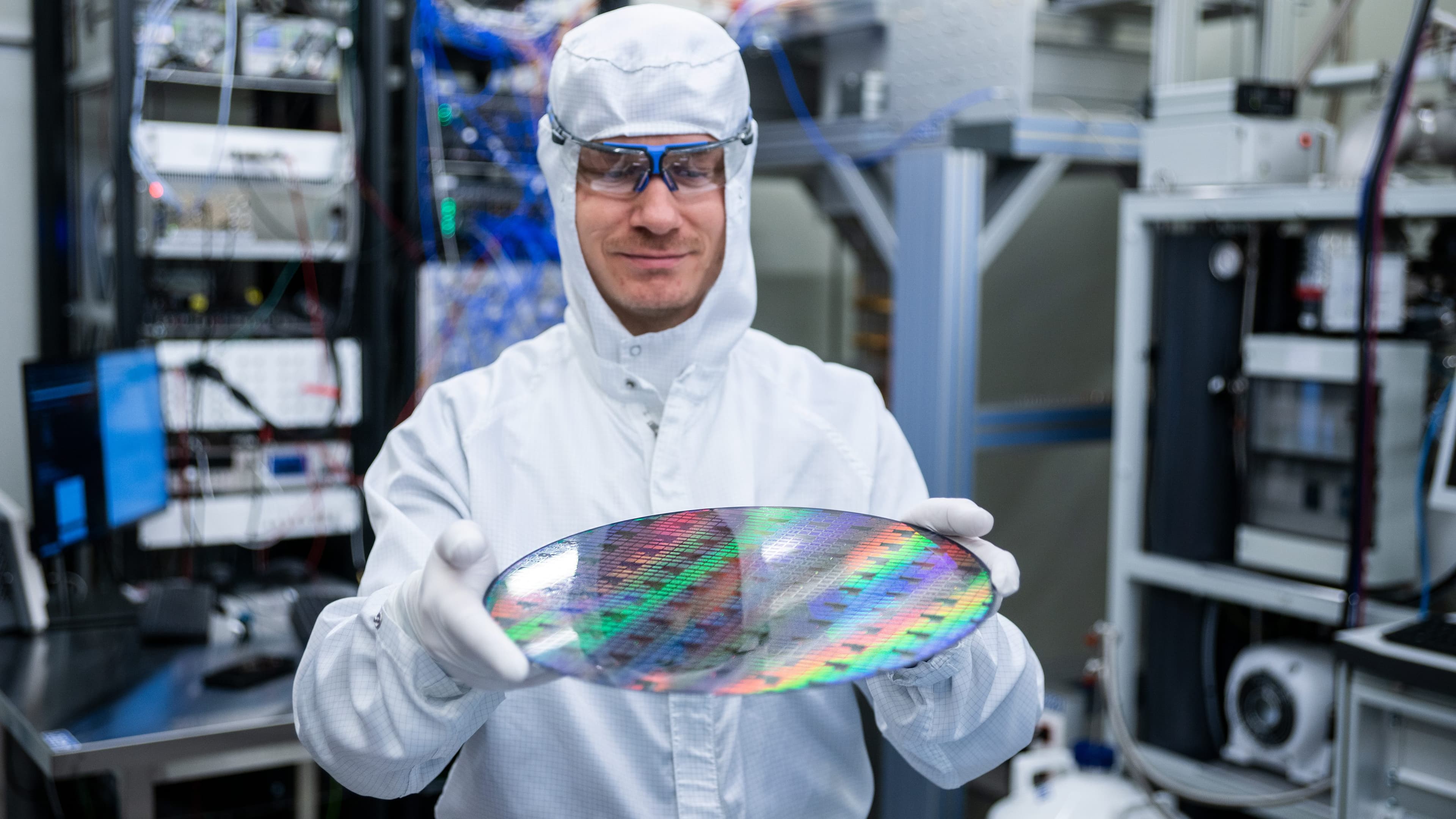
Besides leading the SPINS consortium, imec will focus on technology exploration for the Ge/GeSi platform on 300 mm wafers, with the eventual goal of enabling access through research grade MPW runs and early stage PDK development, supported by wafer level sanity checks and advanced heterogeneous integration capabilities.
Imec’s contribution to SPINS builds on a proven track record in semiconductor quantum research, including record fidelities in silicon quantum dot qubits manufactured with imec’s 300mm process flow (https://www.nature.com/articles/s41586-025-09531-9), the first introduction of EUV lithography in Si MOS quantum dot qubits (IEEE IEDM 2025 | 15-5 | 300mm fabrication of silicon quantum dot spin qubits using 0.33NA EUV lithography) and record-low charge noise in Si MOS quantum dots fabricated on a 300mm CMOS platform (https://www.nature.com/articles/s41534-024-00864-3). Imec also leverages its deep involvement with the academic and industrial ecosystem and collaborations such as the Chips JU project ‘Arctic’ (2024-2027) which, coordinated by imec, is poised to develop scalable cryogenic ICT microsystems and control technology for quantum processors.
Co-funding is provided by the Flemish Government.
From Czech Republic
AMIRES, The business innovation management institute, z.ú.
AMIRES will play a pivotal role in business development, engaging stakeholders, and building a robust ecosystem. Additionally, AMIRES will be instrumental in dissemination and communication activities, ensuring the project's achievements reach a wide audience.
National co-funding for the Czech partners is provided by Ministry of Education, Youth and Sports, Czech Republic.
From Finland
VTT Technical Research Centre of Finland, the University of Jyväskylä, and SemiQon Technologies.
VTT's primary contributions include process and module development for spin qubits on the FD-SOI platform, alongside device modelling and developments for ultra-low drive voltage cryo-electronics. Additionally, VTT is responsible for leading the Process Development and Module Optimization work package. The University of Jyväskylä is primarily involved in the characterization and metrology of qubit devices, with the aim of establishing a high-volume qubit characterization framework together with other partners. SemiQon will lead the development of ultra-low-power cryo-CMOS technology, as well as industrialization and technology roadmap activities.
National co-funding for the Finnish partners is provided by Innovaatiorahoituskeskus Business Finland.
From France
CEA-Leti, Quobly and C12.
CEA will lead activities on Process Design Kits (PDKs) development and Multi-Project Wafer (MPW) execution. It will contribute to achieving foundry compatible FDSOI processes executed on 300 mm platforms in collaboration with Quobly and STMicrolectronics and on superconducting layers to include in BEOL processes. Besides, CEA will lead physics-based device modelling activities to optimize Ge/GeSi heterostructures for device performance. CEA will also design and characterize co-integrated standard circuits working at cryogenic temperatures using industrial CMOS FDSOI technologies. Finally, CEA will be involved in high-volume characterization at 1-4K.
National co-funding for the French partners is provided by ANR, BPI & France 2030.
From Germany
ARQUE Systems GmbH, Forschungszentrum Jülich GmbH, Fraunhofer, IHP, Infineon, Siltronic and the University of Regensburg.
The German contribution will be on industrial semiconductor qubit technology based in Si/SiGe heterostructures. It will build on results from projects QUASAR (funded by the German Ministry of Research, Space and Technology) and EU Flagship projects QLSI and QLSI2, to turn qubit device fabrication processes into a reproducible, well-documented and accessible technology. Fabrication will be carried out at IHP and Siltronic (heterostructure substrates), Infineon Dresden (overall technology and process integration) and Fraunhofer IPMS (electron beam lithography and qubit-adapted packaging). These contributions will be complemented with characterization work at Forschungszentrum Jülich GmbH, Fraunhofer IAF, the University of Regensburg and ARQUE Systems GmbH.
From Italy
National Quantum Science and Technology Institute (NQSTI)
NQSTI will contribute electrical characterisation of devices at cryogenic temperatures: within WP5, heterostructure-based devices (e.g., HEMTs) will be investigated up to microwave frequencies, targeting cryoelectronic solutions for qubit control and readout. Within WP6, qubits implemented in SOI and Ge platforms will be characterised at their operating temperatures (<1 K).
National co-funding is provided by the Italian Ministry of University and Research (MUR)
From The Netherlands
Groove Quantum, QuTech, TNO and TU Delft.
Developing the pilot line and the PDK requires careful testing of devices using common standards, as it allows the pilot line to be evaluated and improved efficiently. Groove Quantum’s main focus is to set up and coordinate a high-throughput measurement effort at extremely low, quantum-relevant temperatures. This allows to provide fast feedback to guide further development of the pilot line.
The Dutch partners thank Quantum Delta NL and the Rijksdienst voor Ondernemerschap (RvO) for the national support behind the launch of this project.
From Portugal
The International Iberian Nanotechnology Laboratory (INL) and the Portuguese Quantum Institute (PQI).
INL contributes expertise in semiconductor process integration, quantum device characterization, and cryogenic testing to support spin qubit validation and MPW development.
PQI will be analysing comprehensively the energetic performance of semiconductor quantum bits and quantum chips, and addressing the corresponding benchmarking and improvement.
From Spain
Quantum Motion Spain and Consejo Superior de Investigaciones Científicas (CSIC)-Instituto de Microelectrónica de Barcelona (IMB-CNM).
Quantum Motion Spain will study monolithically integrated electronics and qubits and, particularly, how power dissipation may impact qubit performance. As an output, QMS will develop a predictive modelling capability for thermal flow with the aim to minimise thermal flow and facilitate monolithic integration.
CSIC participates in process development and module optimization. The objective is to gather and unify the required development of key process steps and modules that are currently not available and need to be developed to meet the requirements of a stable semiconductor pilot line adapted to the needs of the quantum industry. CSIC contributes with the cleanroom capabilities of the IMBCNM to implement improvements in the gate stack module.
National co-funding for the Spanish partners is provided by the Ministry for Digital Transformation and Public Service.
About imec
Imec is a world-leading research and innovation hub in advanced semiconductor technologies. Leveraging its state-of-the-art R&D infrastructure and the expertise of over 6,500 employees, imec drives innovation in semiconductor and system scaling, artificial intelligence, silicon photonics, connectivity, and sensing.
Imec’s advanced research powers breakthroughs across a wide range of industries, including computing, health, automotive, industry, consumer electronics, aerospace and security. Through IC-Link, imec guides companies through every step of the chip journey - from initial concept to full-scale manufacturing - delivering customized solutions tailored to meet the most advanced design and production needs.
Imec collaborates with global leaders across the semiconductor value chain, as well as with technology companies, start-ups, academia, and research institutions in Flanders and worldwide. Headquartered in Leuven, Belgium, imec has research facilities in Belgium, across Europe, the USA and the GCC region, and representation on three continents. In 2024, imec reported revenues of €1.034 billion.
The imec group holds a global trademark portfolio, including word marks and combined figurative registered and unregistered trademarks, across national, regional, and international territories. Its lawful use requires prior written consent of IMEC in compliance with the IMEC branding guidelines, which may be updated periodically. The latest version is available upon written request.
Discover more
Anton Potočnik receives prestigious ERC Consolidator Grant to enable scalable superconducting quantum computers with qubit readout at near absolute zero (milliKelvin) temperatures
Read more
New leap in Belgian quantum communication infrastructure: imec, UGent and Belnet realize first QKD links
Read more