Europractice 2.0 secures EU funding until September 2028
Affordable chip design tools, MPW services and training to empower research and innovation across Europe.

LEUVEN (Belgium), February 12, 2026 – A consortium of five European partners, coordinated by imec, has secured European funding for Europractice services until September 2028. Funded by Chips JU, Europractice 2.0 will sustain and extend the trusted, long-standing Europractice services that have enabled world-class chip design and prototyping for academia, research institutes, and their spinouts over the past 30 years.
Launched in 1995, Europractice supports more than 600 European universities and research institutes every year. It provides users with a full range of services needed to design and fabricate electronic circuits and smart integrated systems. This includes affordable access to industry-standard design tools, fabrication technologies, training, and full technical support. The Europractice consortium is led by imec and includes UKRI-STFC, Fraunhofer IIS, Grenoble INP-UGA, and Tyndall National Institute.
Europractice 2.0 will extend these well-established Europractice services to address new challenges and further support Europe’s semiconductor sovereignty. It will offer fabrication services in more than 90 technologies from various suppliers based on the cost-sharing multi-project wafer (MPW) principle, complemented by packaging and heterogeneous integration techniques.
The portfolio will be continuously updated with advanced and emerging technologies including those from European research centres and Chips JU pilot lines. To expedite the design process, the project will facilitate design IP exchange within the user community.
Addressing Europe’s semiconductor skills gap remains a core mission. Europractice 2.0 will train more than 650 participants annually, amplifying its impact through a train-the-trainer initiative. Simplified design flows and shared tapeouts for ClassIC student chips – aimed specifically at undergraduate students – will further lower entry barriers and expand hands-on learning.
Europractice 2.0 will also nurture early-stage academic spinouts during their incubation phase. Close collaboration with the EU Chips Design Platform (EuroCDP) will ensure a seamless transition to acceleration and commercialization, creating a clear, structured path from research to market and contributing to the long-term growth and competitiveness of Europe’s semiconductor ecosystem.
The Europractice 2.0 project is supported by the Chips JU and its members under grant agreement nr.101252350.
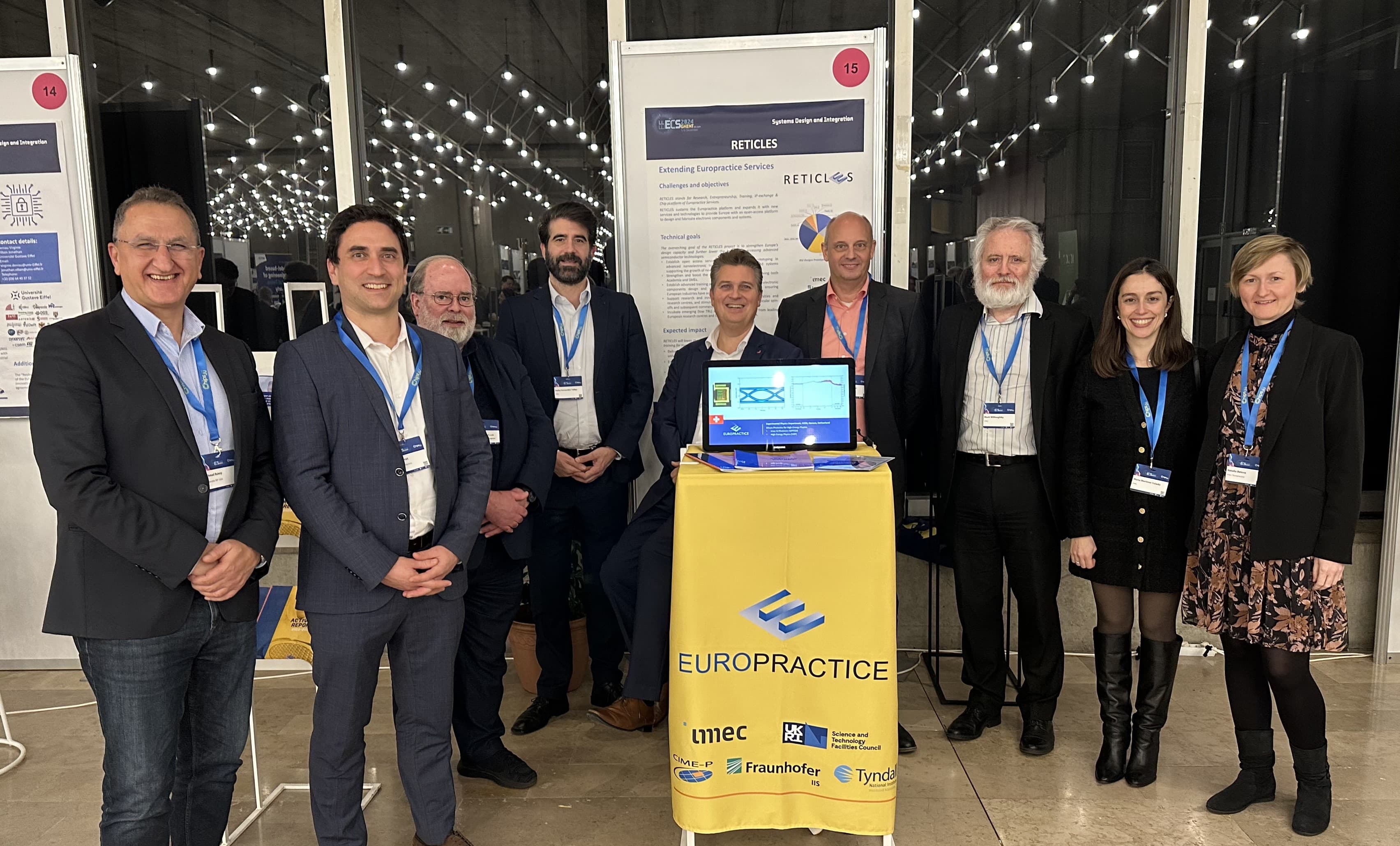
About Europractice
Europractice lowers the barriers to the design and fabrication of electronic circuits and systems, serving more than 600 European universities, research institutes, and their spinouts each year. Acting as a one-stop shop, it provides users with easy and affordable access to industry-standard design tools, prototype fabrication services, and an extensive portfolio of in-depth, hands-on training courses.
For more than 30 years, Europractice has continuously expanded its technology portfolio, which today spans a wide range of offerings, from ASICs and compound semiconductors to photonics, flexible electronics, graphene, and more.
Europractice is a consortium of five partners: imec (Belgium), UKRI-STFC (UK), Fraunhofer IIS (Germany), CIME-P/Grenoble INP (France), and Tyndall National Institute (Ireland). Over the years, Europractice services have been sustained and extended thanks to the support of the European Commission, currently via the Chips JU project Europractice 2.0.

About imec
Imec is a world-leading research and innovation hub in advanced semiconductor technologies. Leveraging its state-of-the-art R&D infrastructure and the expertise of over 6,500 employees, imec drives innovation in semiconductor and system scaling, artificial intelligence, silicon photonics, connectivity, and sensing.
Imec’s advanced research powers breakthroughs across a wide range of industries, including computing, health, automotive, energy, infotainment, industry, agrifood, and security. Through IC-Link, imec guides companies through every step of the chip journey - from initial concept to full-scale manufacturing - delivering customized solutions tailored to meet the most advanced design and production needs.
Imec collaborates with global leaders across the semiconductor value chain, as well as with technology companies, start-ups, academia, and research institutions in Flanders and worldwide. Headquartered in Leuven, Belgium, imec has research facilities in Belgium, across Europe and the USA, and representation on three continents. In 2024, imec reported revenues of €1.034 billion.
For more information, visit www.imec-int.com
The imec group holds a global trademark portfolio, including word marks and combined figurative registered and unregistered trademarks, across national, regional, and international territories. Its lawful use requires prior written consent of IMEC in compliance with the IMEC branding guidelines, which may be updated periodically. The latest version is available upon written request.
Discover more




Anton Potočnik receives prestigious ERC Consolidator Grant to enable scalable superconducting quantum computers with qubit readout at near absolute zero (milliKelvin) temperatures
Read more
Imec inaugurates its Baden-Württemberg office, focused on advancements in automotive chiplet
Read more