Imec Introduces Intermetallics and Airgaps in Advanced Interconnect Metallization Schemes
At IITC 2021, imec lays out interconnect options for beyond 1nm technology nodes
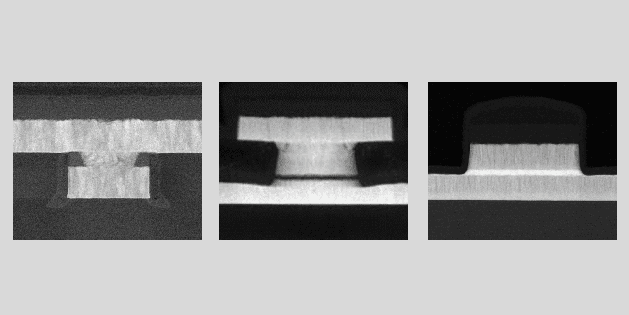
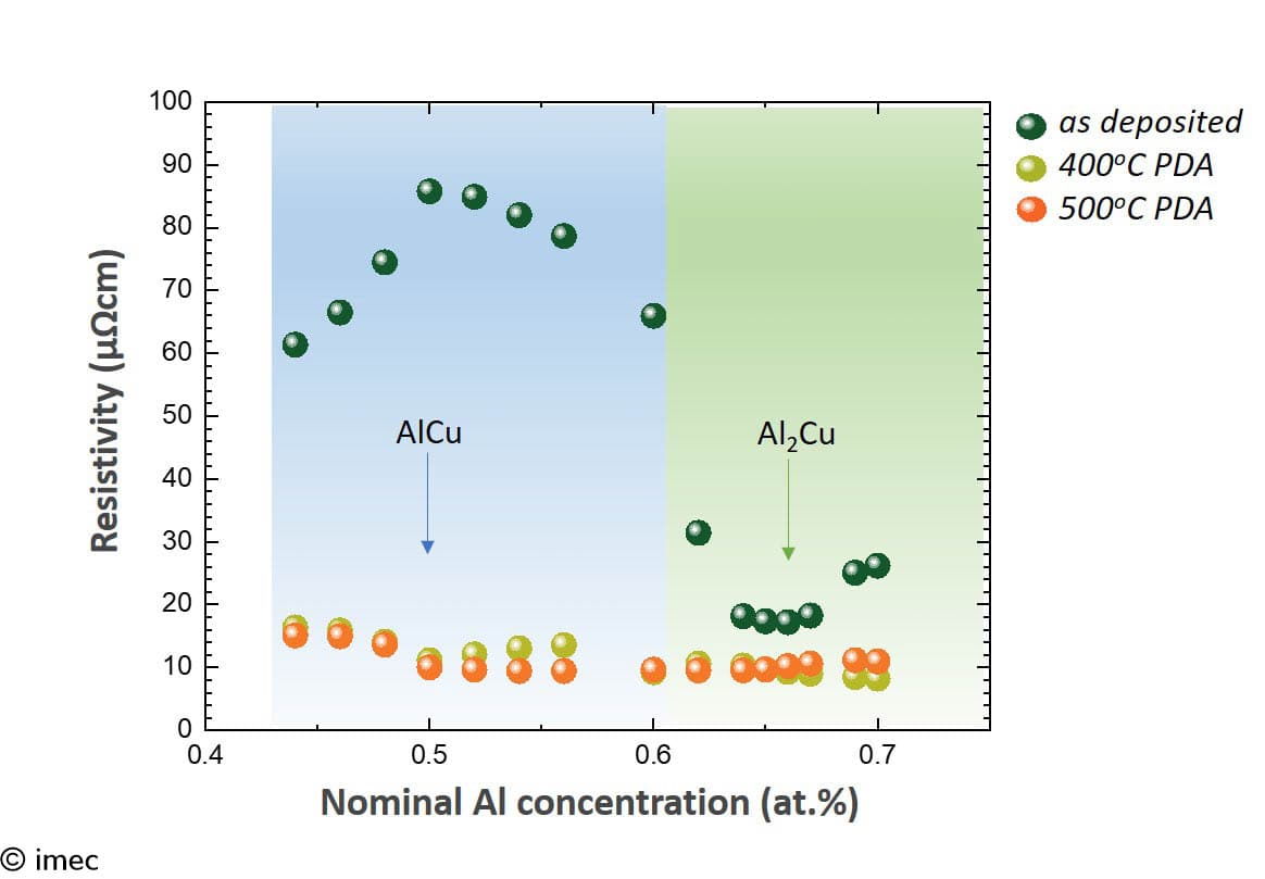
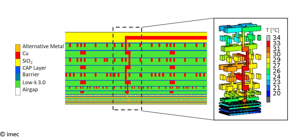
LEUVEN (Belgium), July 06, 2021— This week, at the 2021 International Interconnect Technology Conference (IITC 2021), imec, a world-leading research and innovation hub in nanoelectronics and digital technologies, presents an experimental study of Al-based binary compounds, with focus on their resistivity behavior. For example, for stoichiometric AlCu and Al2Cu films, a resistivity as low as 9.5µΩcm was reported. These results experimentally support their promise to be used as new conductors in advanced semi-damascene interconnect integration schemes, where they can be combined with airgaps for improved performance. In this combination, however, Joule heating effects are becoming increasingly important. This was predicted by combined experimental and modeling work in a 12-layer back-end-of-line (BEOL) structure – implementing new metals and airgaps.
Scaling down the logic technology roadmap to 1nm and beyond will require the introduction of new conductor materials in the most critical layers of the back-end-of-line. Of interest are binary and ternary intermetallic compounds (e.g., Al or Ru based) with lower resistivity than conventional elemental metals (such as Cu, Co, Mo or Ru) at scaled dimensions. Imec has experimentally investigated the resistivity behavior of thin films of aluminides, including AlNi, Al3Sc, AlCu and Al2Cu. At 20nm thickness and above, all PVD-deposited films showed resistivities comparable to or lower than Ru or Mo. The lowest resistivity of 9.5µΩcm was achieved for 28nm films of AlCu and Al2Cu – a value that goes below that of Cu. The experiments also indicated challenges for the studied aluminides, such as the control of the film stoichiometry and surface oxidation.
Imec envisions to introduce intermetallic compounds in advanced semi-damascene integration schemes, which involve the direct etch of a patternable metal to achieve higher aspect ratio lines. Further improvements in RC delay can be obtained by gradually introducing partial or full airgaps in between the metal lines. Replacing conventional low-k dielectrics with electrically isolating airgaps is expected to reduce capacitance at scaled dimensions. But airgaps have an extremely poor thermal conductivity, which raises concerns for Joule heating at operation conditions.
Imec has quantified this challenge by performing Joule heating ‘calibration’ measurements at local 2-layer metal interconnect level and projecting the results to a 12-layer BEOL structure through modeling. The study predicts a 20% increase in temperature with airgaps. The density of the metal lines was found to play an important role: higher metal density showed to help reducing the Joule heating.
“These insights are key to improve semi-damascene metallization schemes as an interconnect option for 1nm and beyond,” says Zsolt Tokei, imec fellow and program director of nano-interconnects at imec. “Besides, imec is expanding the interconnect roadmap with other options, including hybrid metallization and new middle-of-line schemes, while solving critical challenges related to process integration and reliability. These and other topics are presented at this year’s IITC in 9 papers, illustrating the impact of our global R&D efforts to create solutions for sub-2nm interconnect scaling.”
About imec
Imec is a world-leading research and innovation center in nanoelectronics and digital technologies. Imec leverages its state-of-the-art R&D infrastructure and its team of more than 4,500 employees and top researchers, for R&D in advanced semiconductor and system scaling, silicon photonics, artificial intelligence, beyond 5G communications and sensing technologies, and in application domains such as health and life sciences, mobility, industry 4.0, agrofood, smart cities, sustainable energy, education, … Imec unites world-industry leaders across the semiconductor value chain, Flanders-based and international tech, pharma, medical and ICT companies, start-ups, and academia and knowledge centers. Imec is headquartered in Leuven (Belgium), and has research sites across Belgium, in the Netherlands, Taiwan and the USA, and offices in China, India and Japan. In 2020, imec's revenue (P&L) totaled 680 million euro.
Further information on imec can be found at www.imec-int.com.
Imec is a registered trademark for the activities of imec International (IMEC International, a legal entity set up under Belgian law as a “stichting van openbaar nut”), imec Belgium (IMEC vzw supported by the Flemish Government), imec the Netherlands (Stichting IMEC Nederland), imec Taiwan (IMEC Taiwan Co.), imec China (IMEC Microelectronics (Shanghai) Co. Ltd.), imec India (IMEC India Private Limited), imec San Francisco (IMEC Inc.) and imec Florida (IMEC USA Nanoelectronics Design Center Inc.).
Discover more

A double world-first: integrating lithium niobate and lithium tantalate modulators on silicon photonics through micro-transfer printing
Read more
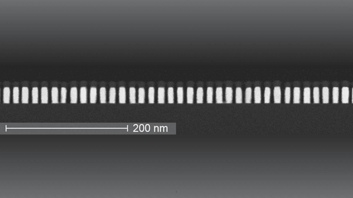
Imec demonstrates 16nm pitch Ru lines with record-low resistance obtained using a semi-damascene integration approach
Read more