Improved quantum-device characteristics in a semi-industrial process flow
Imec shows uniform and tunable all-silicon spin qubit devices in a 300mm integrated process flow.

In short
At VLSI 2021, imec presents its progress in the device characteristics of electron-spin qubits in terms of the uniformity and tunability needed to create qubits arrays for computing purposes.
In parallel, an all-silicon approach is adopted to increase thermal compatibility at cryogenic temperatures.
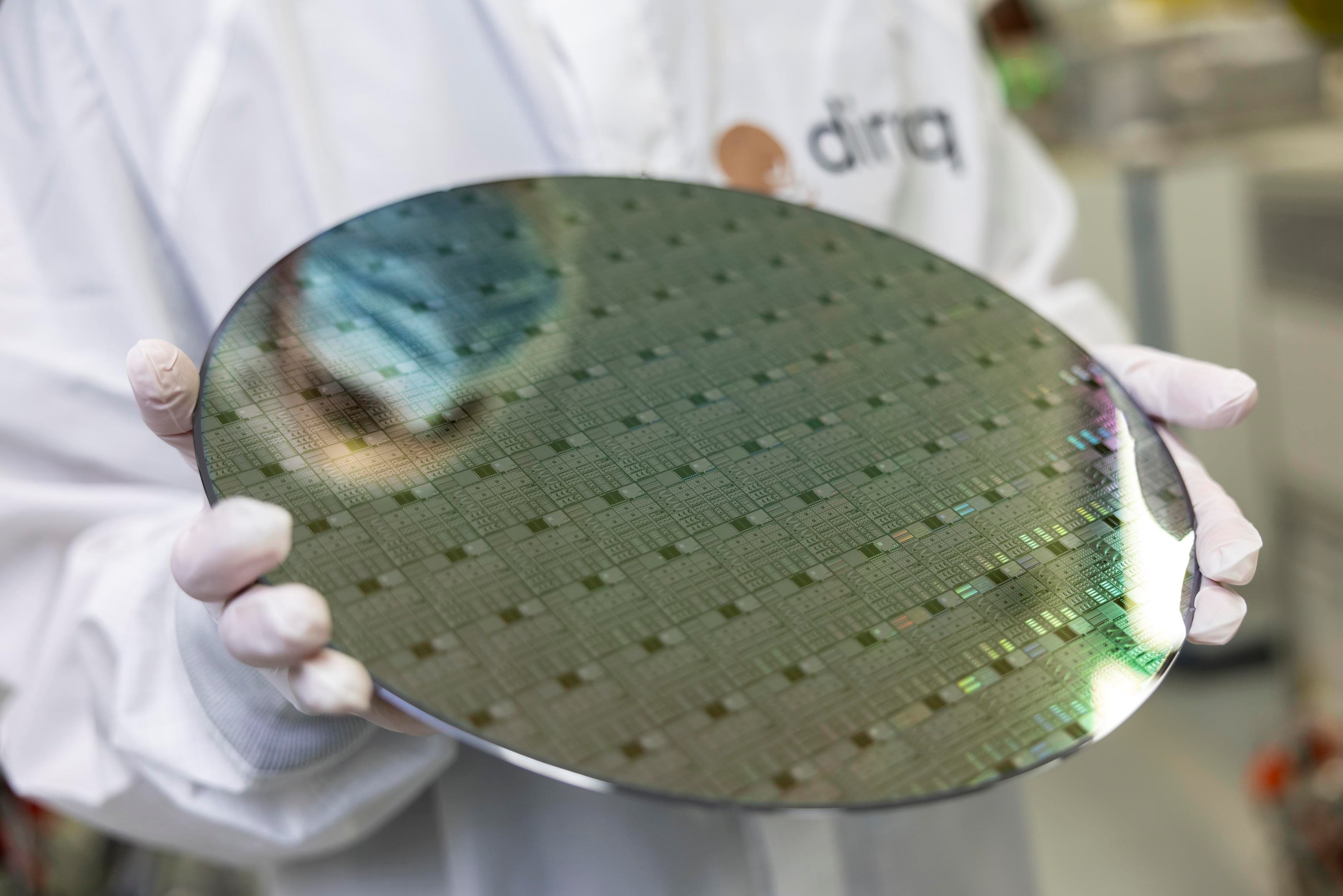
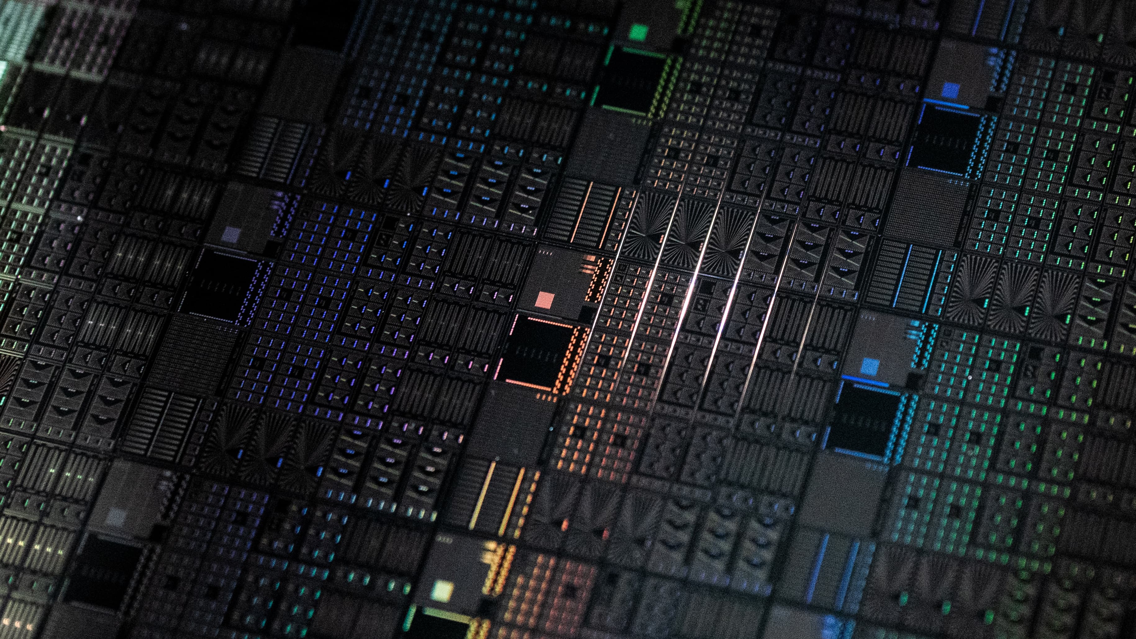
The devices are produced in imec’s dedicated 300mm process flow, which supports future industrial compatibility.
In the global pursuit of quantum computing, the unknowns still largely outnumber the aspects of certainty. While it is too early to assess which of the many technology options will prove to be the winning candidate in final applications, important strides forward are being made on each of the explorative routes. In one of these routes, namely spin qubits, imec used its semi-industrial 300mm process flow to create qubit devices, of which some important characteristics match lab-based results. Imec presents this positive improvement at the renowned 2021 Symposia on VLSI Technology and Circuits (June 13-19).
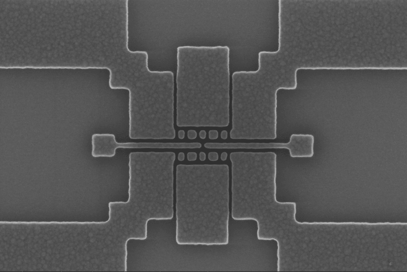
One of the challenges in quantum computing is to achieve high uniformity in qubit arrays to lower noise and improve coupling between individual qubits. One way to overcome the challenge is by improving process control. For the first time, imec realized an array of electron-spin qubits with high uniformity and low charge-noise levels of 3.6µ√Hz at 1Hz; which matches lab-scale results.
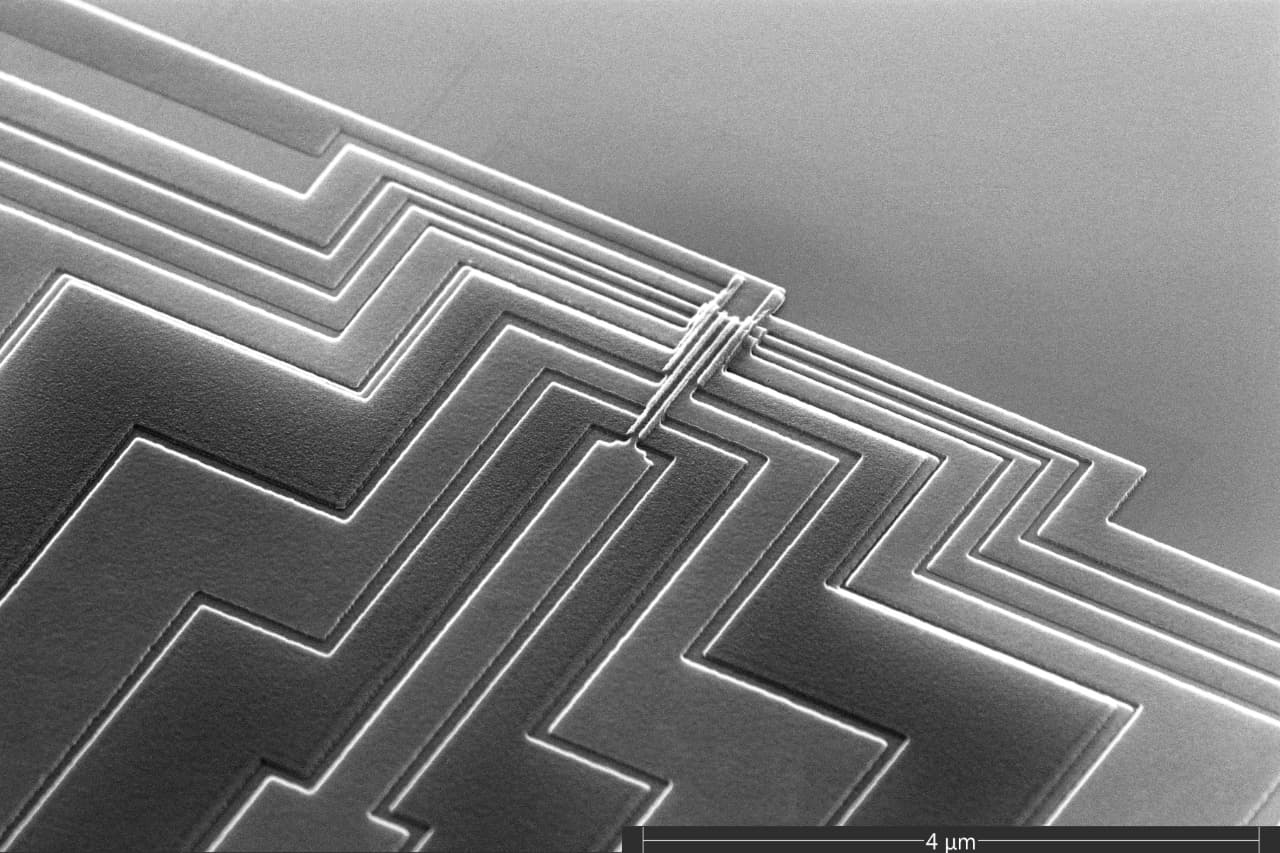
In parallel to the 300mm process integration, imec also introduced some new design choices. Notably, researchers made an important change in the material stack. Where they previously used TiN in the gate stack, they opted for a novel overlapping polycrystalline silicon gate stack instead. This ‘all-silicon’ approach should be beneficial for the thermal compatibility at cryogenic temperature because of fewer strain-related disorders, as was confirmed by uniform Vth distributions collected on randomly selected test transistors for temperatures down to 8milliKelvin.
Additional features that showed excellent results were the interface mobility, plus the interdot-coupling control and its reproducibility. Very large mobilities of up to 15,000cm2/Vs were measured at a temperature of 10Kelvin. These mobilities match state-of-the-art and are an important parameter for the low number of device impurities and defects. For reference, traditional silicon transistors have a mobility of 70 cm2/Vs at room temperature.
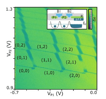
Researchers also demonstrated reproducible and symmetric tunnel-coupling (tc) control up to 100GHz over nearly two decades (2-100GHz). This is an important indicator of how well adjacent qubits can be connected to each other and operated, a must-have for building qubit arrays.
These low-disorder, uniform qubit devices and 300mm fab integration pave the way for fast scale-up to large quantum processors. Imec warmly welcomes industrial partners, startups as well as established players, to set up partnerships and actively join in on further research and development. Full details of these latest achievements can be found in the VLSI paper (JFS5 & Technology / Circuits Joint Focus Session 5 - Circuit and Technology for Quantum Computing – scheduled Saturday, June 19, 2021).
Want to know more?
- Request the VLSI paper “Uniform Spin Qubit Devices with Tunable Coupling in an All-Silicon 300 mm Integrated Process” (Dumoulin et al.) – Contact form
- An overview of the main research tracks in quantum computing: About qubits and quantum circuits | imec (imec-int.com)
- More details on the 300mm platform and the associated research challenges: Moving Quantum Computing from Lab to Fab | imec (imec-int.com)
Authors

Iuliana Radu
Iuliana Radu is program director at imec, where she is leading the beyond CMOS and quantum computing activities. Prior to joining the logic program at imec in 2013, she was a Marie Curie and FWO fellow at KU Leuven and imec. Her work at imec and KU Leuven includes devices using the metal-to-insulator transition, ionic and electronic transport in functional oxides and devices with graphene and other 2D materials. Iuliana has received a PhD in physics from MIT in 2009 where she worked on the fractional quantum Hall effect and searched for non-abelian quasiparticles.

Bogdan Govoreanu
Bogdan Govoreanu is Quantum Computing Program Manager at imec, where he coordinates the technical research and development program activities. Prior to this, his research work included various topics in Memory Technology and Emerging Devices, with focus on Flash and resistive switching memory technologies, selectors and neuromorphic computing. He developed strong interests in novel concepts for computing and storage beyond current mainstream technologies. As of 2017, his research focuses on Quantum Computing Technologies and Systems. Bogdan holds a Ph.D. degree in Applied Sciences from KU Leuven for his research performed at imec on novel tunnel barrier concepts.
Discover more

Imec and Diraq demonstrate first coherent operation of eight silicon MOS spin qubits fabricated in a 300mm CMOS-compatible foundry process
Read more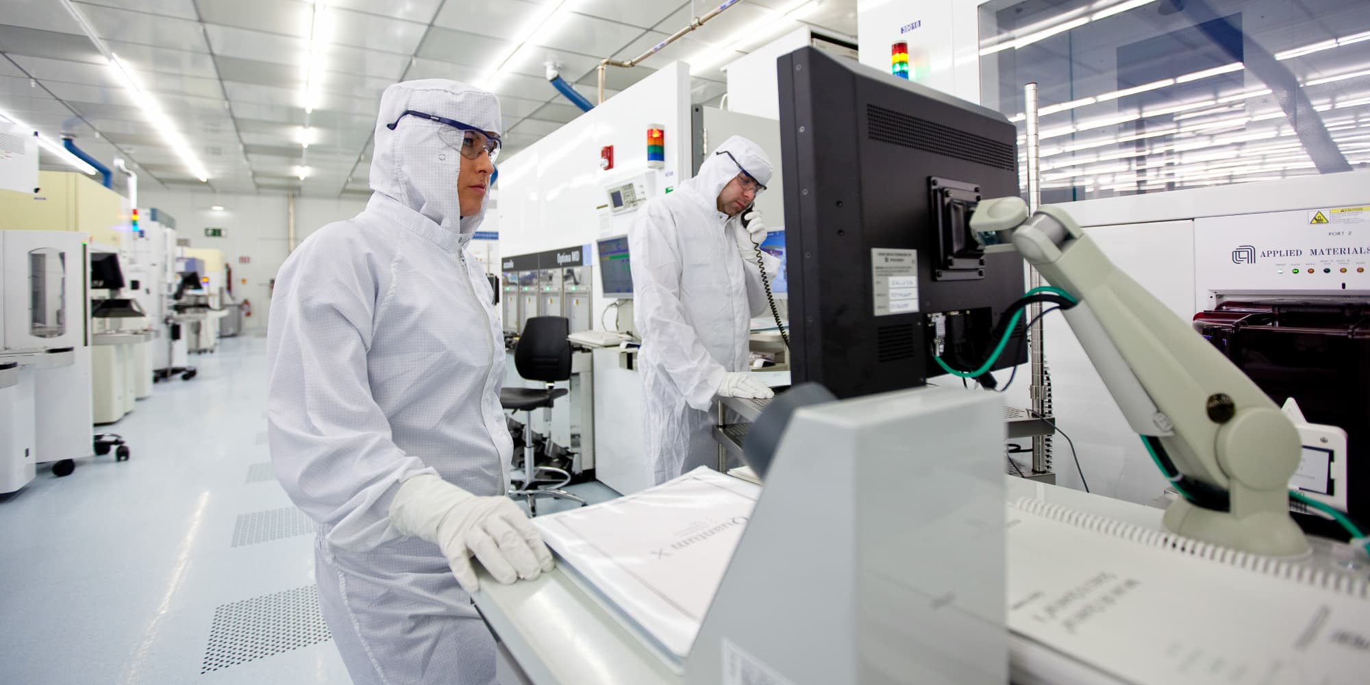


Anton Potočnik receives prestigious ERC Consolidator Grant to enable scalable superconducting quantum computers with qubit readout at near absolute zero (milliKelvin) temperatures
Read more