Moving Quantum Computing from Lab to Fab
Imec Presents 300 mm Platform for Silicon Spin Qubit Design

In short
At the IEEE International Electron Devices Meeting (IEDM2020), imec demonstrates the first flexible hardware platform for silicon spin qubit integration on 300 mm wafers.
Imec also proposes novel ways to operate multiple qubits in a linear array and to combine classical electronics with quantum circuits at low temperatures.
These are significant steps forward in the development of large-scale silicon quantum processors, highlighted as a key emerging technology on IEDM.
What technology will the future quantum computer be built on? There is no clear winner in the quantum race yet. The development of the first generation of commercial quantum computers mainly relies on superconducting qubits or trapped ions, but quantum computers based on semiconductor spin qubits are making great strides. The last few years, silicon-based quantum-dot systems have demonstrated long coherence times and high-fidelity operation in laboratory settings. Silicon-based qubits are attractive for potential use in large-scale quantum processors because they are compatible with the technology handled by the microchip industry for over half a century. These well-established processes enable high volume manufacturing, which makes semiconducting qubits convenient in terms of scalability. But scaling up existing qubit prototypes to several qubit arrays requires advanced fabrication techniques.
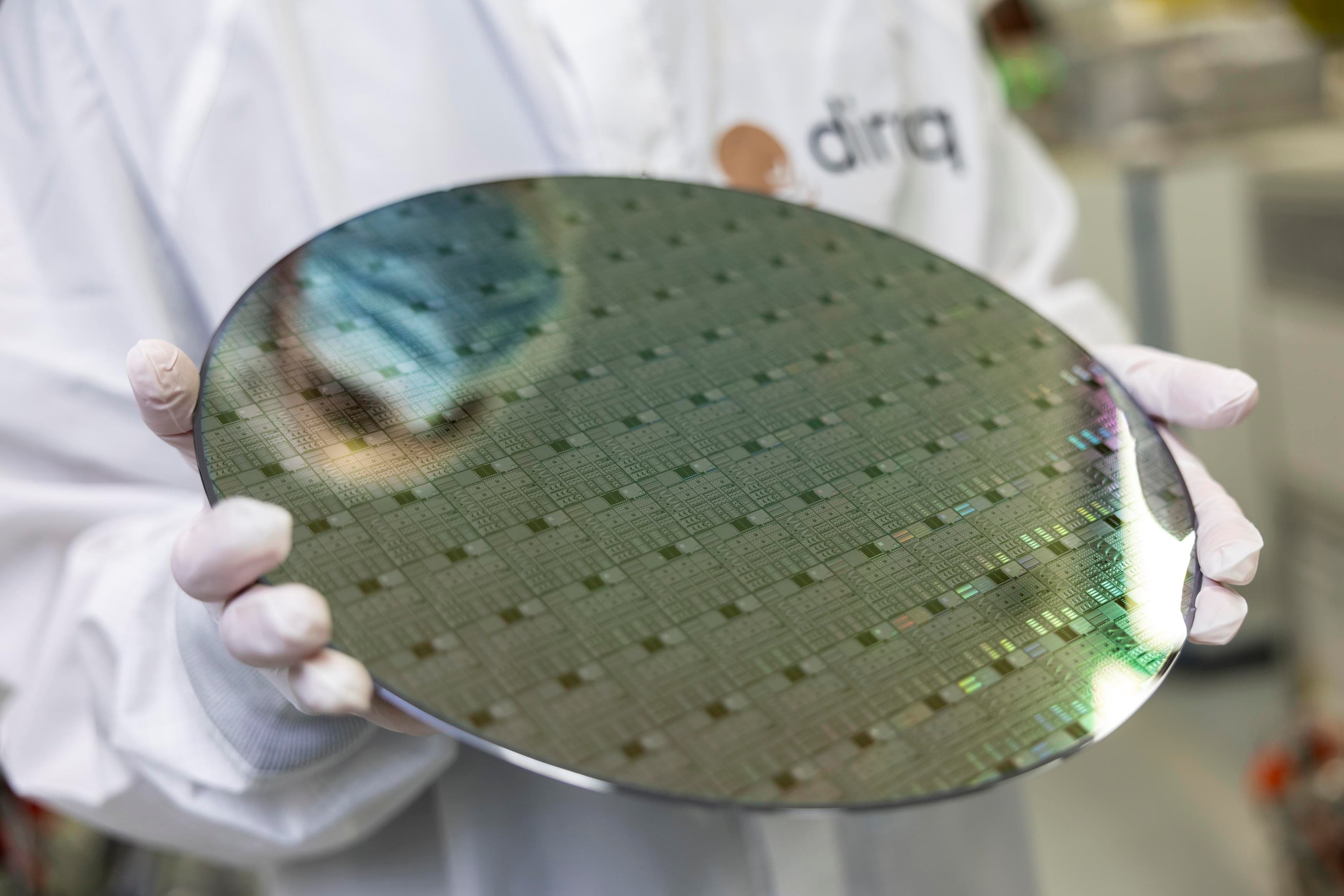
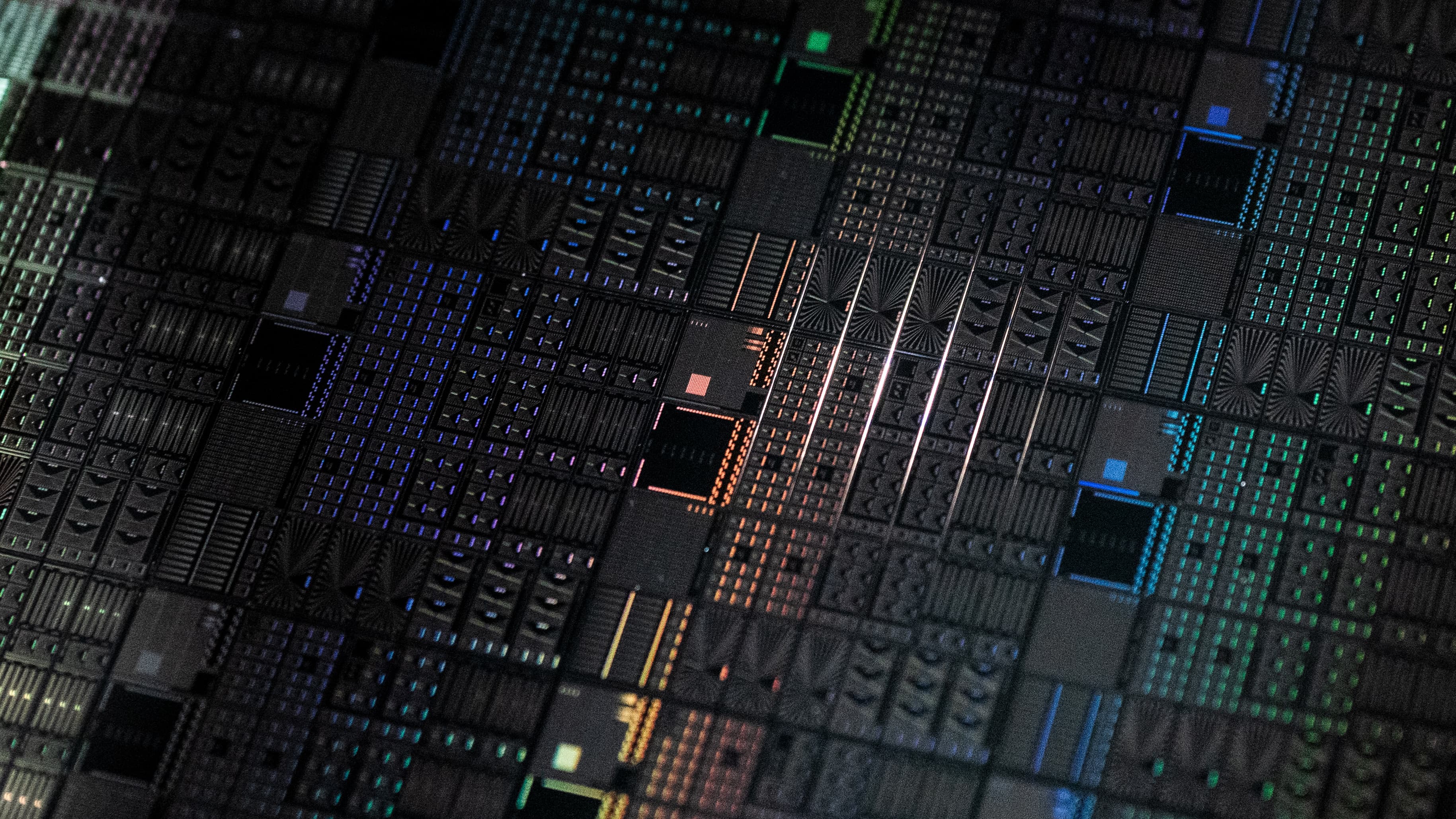
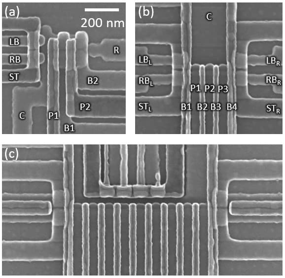
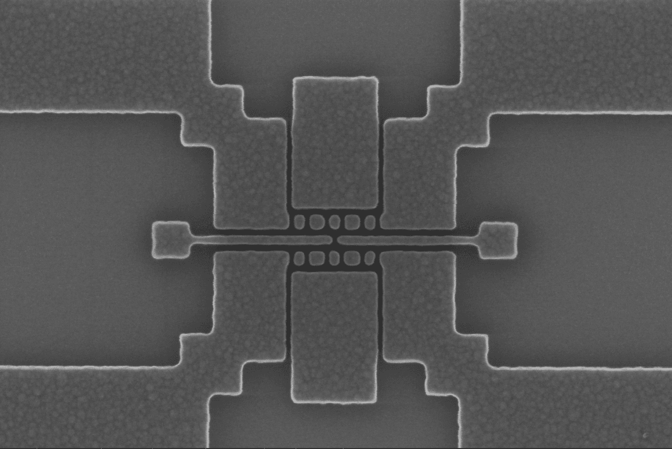
To address this challenge, imec has leveraged its 300 mm fab expertise and developed a process that optimally combines optical and electron beam lithography to fabricate silicon spin qubits. The design platform is based on industry standard 300 mm silicon wafer fabrication technology instead of specialized laboratory processes. The shift from lab to fab happens without losing any flexibility: the platform enables on-the-fly layout design modifications. This flexibility allows to incorporate different structures across the 300 mm wafer, from a double quantum dot device to a one-dimensional qubit array, as shown in Fig 1. “The 300 mm fabrication platform is the first versatile hardware toolbox that allows such flexible qubit device designs”, says Iuliana Radu, program director at imec, where she is leading the quantum computing activities.
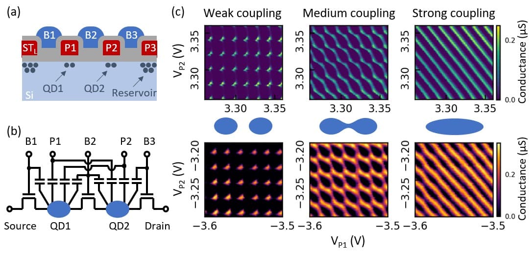
The flexible integration platform for silicon spin qubits is presented in a focus session on key emerging technologies on IEDM 2020. The imec researchers demonstrate the ability to manipulate individual quantum dots from external circuits, as shown in Fig. 2. “If an electron is trapped in one of the quantum dots, we can manipulate it with an RF signal. We can control the angle at which the spin of the electron is pointing, but we are also able to change the tunnel coupling between adjacent quantum dots. These are prerequisites for qubit operations”, explains Ruoyu Li, device engineer at imec.
By moving the qubit research to a flexible 300 mm fab, a first important step has been taken on the path to the development of large-scale silicon spin quantum processors. “The next step is to use the platform for further study on how to build and how to operate large arrays of qubits”, says Radu. “We are also open for collaboration with start-ups that are interested in exploiting our 300 mm platform to enter the emerging quantum computing industry.”
How to operate a large array of qubits?
Meanwhile, imec’s quantum group is already working on these next steps. Being able to control one qubit does not suffice for large-scale computations, you also need to deal with the physical interaction between that qubit and its nearest neighbors. “Once we can build and measure a large array of qubits, we would need to figure out how to implement logic gates in this array”, explains George Simion, theoretical physicist at imec. To tackle this challenge, he proposed a scalable way to operate multiple qubits in a linear array. The proposal is based on nanomagnets and allows to increase the size of the qubit array while the qubits can still be addressed individually.
Placing classical electronics inside the fridge
Another challenge for building a full quantum computer is the engineering problem of connecting the qubits with classical circuits. The challenge becomes increasingly more difficult with increasing number of qubits, as you might end up with a tangle of millions of input and output-wires. “This wiring problem could be resolved by bringing the classical interface electronics closer to the qubits. This means that some of the classical electronics should be placed in the refrigerator where the qubits reside – operating at milli Kelvin temperature. This has directed research towards interface electronics that can operate at low temperature to drive and read-out multiple qubit-states”, says Jan Craninckx, invited to speak at IEDM about the circuits needed to drive qubits. In an overview paper he describes how nanoscale CMOS transistor properties are conveniently well suited for this task, when properly modelled.
“There is still a lot of research that needs to happen, even on standard CMOS, to build this understanding” concludes Iuliana Radu. “The path towards a useful quantum computer is riddled with obstacles, but step by step we’re moving in the right direction”,
Want to know more?
More details can be found in 3 papers presented at the 2020 IEDM conference:
A flexible 300 mm integrated Si MOS platform for electron- and hole-spin qubits exploration
A Scalable One Dimensional Silicon Qubit Array with Nanomagnets
CMOS Cryo-Electronics for Quantum Computing
Discover more

Imec and Diraq demonstrate first coherent operation of eight silicon MOS spin qubits fabricated in a 300mm CMOS-compatible foundry process
Read more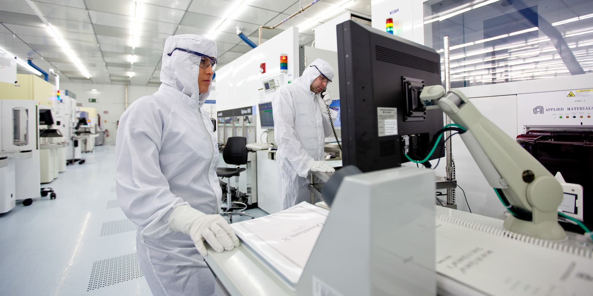


Anton Potočnik receives prestigious ERC Consolidator Grant to enable scalable superconducting quantum computers with qubit readout at near absolute zero (milliKelvin) temperatures
Read more