On-chip optical beamforming
Want to reduce the size and cost of your beamforming application without compromising on power, performance or reliability? Discover imec’s solid-state beamforming technology.

Optical beamforming technology concerns the ability to steer, shape and focus light. It’s a powerful tool to:
- Directly manipulate a light signal, e.g. for LiDAR, optical communication, ...
- Indirectly change a radio frequency on an optical carrier, e.g. for 5G, radar, ...
The market for optical beamforming applications is continuously growing. For example:
- Autonomous vehicles need long-range and high-resolution sensing mechanisms to ensure a safe ride, such as solid-state LiDAR.
- 5G networks require large, flexible bandwidths and directional communication, which can be provided by integrated microwave photonics.
- Free-space optical communication systems demand high-capacity and secure communication links, both via satellites and remote ground links.
- Advanced medical applications, such as OCT scanners, need imaging technologies that enable accurate diagnostics and monitoring.
What do these applications have in common? Their optical beamforming systems need to be compact and low-cost. And that’s where imec’s photonics-based on-chip technology comes in.
Solid-state beamforming technology
Imec’s optical beamforming technology is based on a concept that’s similar to the one used in modern radar systems: a phased antenna array.
Explore more technical details in this article.
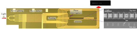
Such a solid-state system is non-mechanical, and therefore reliable, compact and low-power. Moreover, it enables a:
- flexible operational range
- variable resolution
- adjustable communication bandwidth
Features of on-chip optical beamforming
Depending on your application, these optical beamforming features might be essential to you:
- scalability – Imec’s technology is developed in a 200-mm CMOS line. This means low- to high-volume production of functional chips is relatively straightforward.
- flexibility – A photonics-based beamformer is a highly configurable system for communication and range applications. The phase of the carrier frequency can be controlled by true-time delay and phase shifters. And its amplitude can be controlled via a coupling element.
- broadband operation – Flexible and transparent communications subsystems need optical modulators and detectors that cover the whole RF spectrum up to the Ka band. This is easy to achieve with optical components that, unlike their RF counterparts, are intrinsically broadband.
- low power consumption – The move from separately packaged lasers, modulators, detectors, ... to a compact integrated circuit potentially reduces the power consumption of the system. Indirectly, this also relaxes thermal dissipation issues for in-field applications.
- low crosstalk – Channel-to-channel crosstalk and interferences with external sources are minimal in the optical domain.
- small size and low weight – Because integrated photonic circuits bring functionalities like switching, routing, filtering and frequency conversion inside the chip, there’s no need for bulky RF cables and routing mechanisms. This is critical for applications in domains such as space and consumer technology.
Want to discuss the needs of your beamforming application, such as LiDAR or photonics-based image sensors and vision systems?
Download the flyer
Optical beamforming leaflet
DownloadRead more
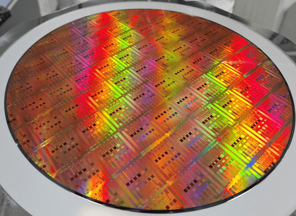
Imec successfully integrates colloidal quantum dot photodiodes (QDPDs) on metasurfaces developed on 300mm CMOS wafers
Pioneering approach makes compact, cost-effective, high-resolution multispectral shortwave infrared (SWIR) sensors accessible, enabling broad application in security, agriculture, automotive, aerospace, and more.
Read more
White paper: monolithic microsystems
Learn how to elevate your application to new heights with advanced functionalities on top of CMOS.
Read more

Imec hyperspectral sensor aboard newly launched earth-observation satellite
The IPERLITE mission is designed to demonstrate next-generation hyperspectral imaging technology in space. At the core is a hyperspectral sensor developed by imec.
Read more