Self-calibrating on-chip optical beamformer reaches high resolution at long distances
Imec presents its on-chip self-calibrating optical beamformer that caters to the next generations of applications such as assisted and autonomous driving, high-resolution earth observation, crop monitoring and flexible high-bandwidth wireless 5G communication.
An increasing number of applications rely on sensors that scan their environment with electromagnetic waves. A key component is accurate beamforming to steer the electromagnetic waves in the right direction.
Imec answers to the industry’s demand for solutions at higher frequencies (e.g. LiDAR) that provide higher resolution and for more reliability by eliminating mechanical moving parts.

The ability to accurately and reliably transmit electromagnetic waves in a controlled direction (aka beamforming) is a crucial enabler for a myriad of applications. Think of 3D scanning applications (e.g. autonomous vehicles and driver-assistance systems, augmented reality, face recognition…) that rely on transmitting electromagnetic waves (RF, light…) accurately and capturing relevant information from their reflections. Or other applications (e.g. high-bandwidth wireless communication such as 5G) for which precise electromagnetic beamforming between sender and receiver is a must. Imec plays a key role in allowing these systems to become more miniaturized and low cost while at the same time increasing their versatility and performance. Xavier Rottenberg, fellow wave-based sensors and actuators at imec, introduces imec’s self-calibrating optical beamformer that allows centimeter precision at hundreds of meters distance.
The market for optical beamforming
There is a vast market for systems that require some sort of beamforming technology. For example, the market for scanning-LiDAR (light-detection and ranging) will - in six years time - double for robotic vehicles, almost double for industrial applications and will even grow a staggering 100-fold (from $19M in 2019 to $1.7B in 2025) for advanced driver-assistance systems (ADAS) (according to a 2020 market report by Yole Development).
Next-generation beamforming technology can create value for high-volume low-cost applications (e.g. 5G, automotive LiDAR…) as well as for low-volume high-cost applications (e.g. spectrometers for medical imaging; earth observation; agricultural crop monitoring…).
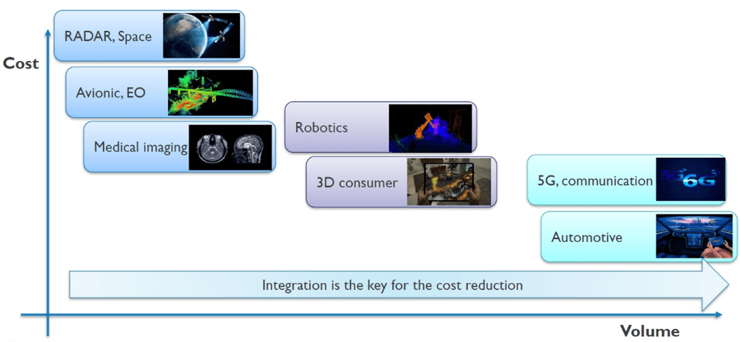
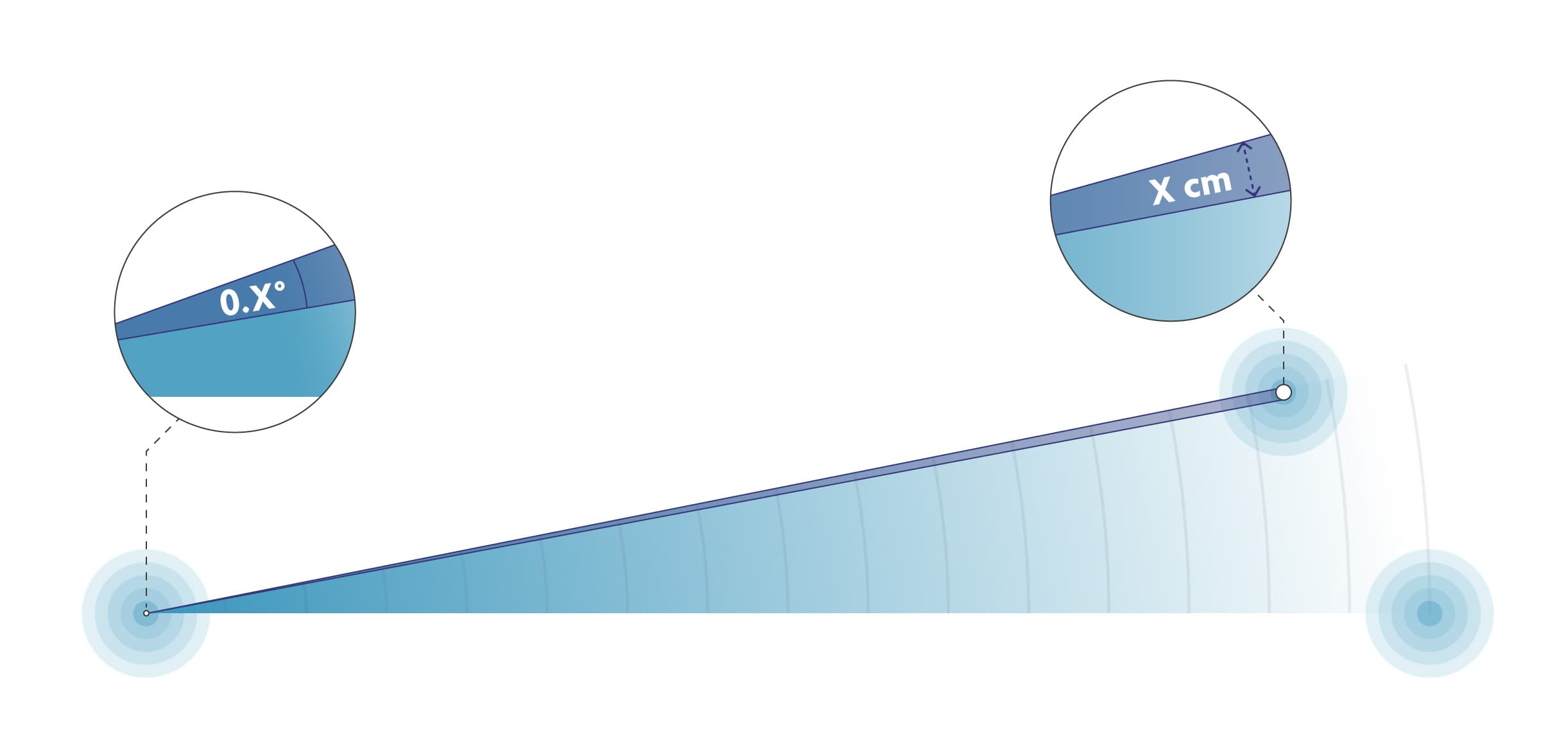
Companies that successfully want to cater to these markets need to tackle several technology challenges first. For instance: how to build devices that achieve the desired resolution at larger distances while maintaining an acceptable form factor? A good example for this accurate transmission and detection is ultra-high bandwidth 5G communication where a precisely directed link shall be established between the central infrastructure and the users to ensure the bitrate and quality of the data transfer. Another example on the ranging domain is when you want to detect and distinguish objects with centimeter-scale precision at distances up to two-hundred meters. This would mean you need to precisely control the transmission angle of the electromagnetic waves with fractions of degrees.
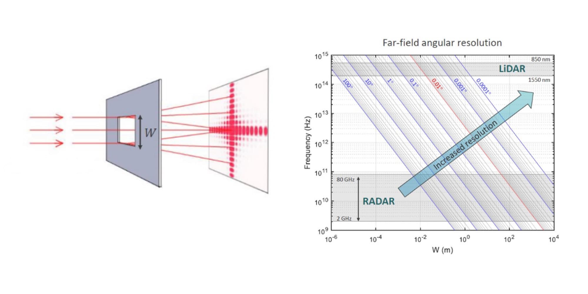
As illustrated in the graph below, the required resolution and the frequency of the applied electromagnetic waves directly impact the required aperture (W) of a system. Doing the math: to obtain a 0,01 degree angular resolution with low-frequency RF signals (radar), one would end up with an aperture of 100x100 meters. These are clearly dimensions that are far from compatible with automotive or satellite applications, if with any application at all.
Move towards higher wavelengths and away from mechanical steering
This pursuit of higher bandwidth and higher accuracies at large distance is the main driver for industry to shift from the RF spectrum to the higher frequency bands of infrared and terahertz imaging. Which for some applications (e.g. humidity control in agrofood) holds the additional benefit of enabling the collection of spectroscopic information such as the chemical composition of surfaces.
Another trend imposed by emerging applications on the LiDAR domain – for example in automotive - is to apply scanning solutions rather than ‘flash’ solutions (which take a full picture of their surroundings in one instance). For the reason that ‘flashing’ an environment in 360 degrees with centimeter precision would at two-hundred meters distance result in a million data points that need to be collected in one go. The power of the light source for such system will be so high that it would drain your battery and blind everyone within close range of your car.
Looking at such scanning systems in low-frequency radar and microwave communication applications, industry increasingly eliminates mechanical parts (such as the radar and phase-array antenna to control the beam steering) and replaces them with digital counterparts for reasons of cost, precision, durability and form factor. That’s why for the described higher-frequency systems, imec immediately steered towards that direction by building a fully digital semiconductor-based optical beamformer with no mechanical parts.
Imec’s self-calibrating optical beamformer
The fact that imec’s solution is fully digital and contains no moving parts immediately is the main differentiator compared to a huge portion of the market. Conventional systems (e.g. mechanical LiDAR) are bulky, costly, need regular maintenance and suffer from reliability issues because of their sensitivity to mechanical shocks and vibrations.
Conceptually, imec’s beamformer is no different than any other: it relies on a waveguide that passes through phase shifters to reach an array of on-chip antennas. Through controlled phase modulation these antennas can transmit signals in a controlled direction. In imec’s latest demonstrators, the beamformer can cover a 40 degree angle (aka field of view, FoV) with below 0.2 degree angular precision. These specifications are not only limited by the enabling design or technology but also can further be improved in the development towards market-ready implementations.
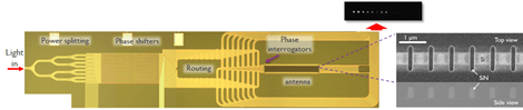
The main novelties of imec’s solution are in the architecture and the choice of material platforms. Where typical solid state lidar systems are built either in silicon or SiN photonics, imec has made a smart combination of both. Building the waveguide and the antennas in SiN to allow for low loss, high-power handling and good process control. And using conventional Si photonics to build the phase shifters and on-chip photodetectors. Si-photonics-based phase shifters are the preferred option over the SiN platform to achieve low-power operation. Because the entire system is compatible with semiconductor manufacturing flows, it allows to drastically reduce the production cost at high volumes.
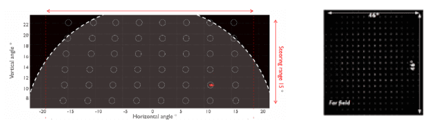
On top of its performance and low-cost-manufacturability potential, the imec solution is self-calibrating via an on-chip solution. This is important, because no matter how precise your system, when processing at the nanometer scale, there will always be slight process and material-related deviations. These result in no antenna or other on-chip building block being 100% identical to its neighbor and inevitably cause deviations in the phase modulation and behavior of the system. As a result, calibration is required to compensate for these inherent aberrations. Normally, such calibration is done in a controlled and complex optical setup that allows to represent what happens if you would send and retrieve signals over distances of hundreds of meters and to correct for the observed deviations. This setup is very unpractical in terms of throughput (when a large number of devices needs calibration) and for use cases where recurring calibration might be needed. As a solution to this problem, imec has embedded on-chip interferometers in between the phase shifters and the antennas. These assess the actual phase difference produced between two adjacent antennas. Measured with integrated photodiodes, this information allows to get an absolute indication of the far-field beam quality, e.g. direction and size, and allows to compensate for non-idealities before the signal gets transmitted. Recently, this technology was used to generate multi-spot sensing by exploiting imec’s design expertise to steer structured-light with a 46-degree field of view in the vertical and horizontal directions.
Wider scope and services
Based on these initial promising results, imec is now looking for application and technology development partners that want to tap into the further development to their specific needs and according to their market constrains. Aside from the optical beamformer, imec can bring in its expertise on advanced process Integration and photonic system design, early access to non-standard device components such as integration of mirrors or high-power lasers. The devices can be produced at various volume levels, either through low-volume manufacturing or, when required, by providing a path to transfer towards foundries with high-volume capacity.
In terms of its own research roadmap, imec will push forward with the beamformer itself; increasing its accuracy and range. But also with the R&D on adjacent components and building blocks that are specific to one or more application domains. For example, a high-speed linear optical modulator for microwave 5G applications is part of the imec roadmap. The heart of the research is carried out to allow for device manufacturing in a 200 or 300mm CMOS line using wafer-scale processes and including electro-optic materials. As such, producing unprecedented components comes within reach at lower cost of production. Also, imec will gradually tackle adjacent components such as the photodetectors for signal detection and the ranging engine that does the computation of incoming data.
These are just a few examples of imec’s aim to widen its offering at the system level. In terms of markets and applications, 3D sensing (and LiDAR in particular) is the most usual suspect and imec’s first target to lead the overall developments. But other domains such as optical telecommunication (LiFi, 5G) are also of imec’s interest and within close reach.
Want to know more?
- Find more details and an insightful movie on our dedicated optical-beamforming webpage
- Check out the imec presentation and conference paper at the SPIE 2020 conference
- In March 2021, Photonics Media reported on this achievement: New Optical Beamformer Designs Spotlight High-End Applications | Industry Insight | May 2021 | Photonics Spectra
Authors

Xavier Rottenberg
Xavier Rottenberg is scientific director and group leader wave-based sensors and actuators at imec. He received the MSc degree in Physics Engineering and a supplementary degree in Theoretical Physics in 1998 and 1999 from "Université Libre de Bruxelles", Belgium. He received further his PhD degree in Electrical Engineering in 2008 from KU Leuven, Belgium. He worked one year at the Royal Meteorological Institute of Belgium in the field of remote sensing from space and joined imec in 2000.

Marcus Dahlem
Dr. Marcus Dahlem joined imec in 2018 as Principal Member of Technical Staff and is currently working on photonic integrated circuits for optical beamforming and optical switching in LiDAR applications. He has (co-) authored over 100 peer reviewed publications. He received his Licenciatura degree (BS + MSc) in Applied Physics from the University of Porto, and his MSc and PhD degrees in Electrical Engineering and Computer Science (EECS) from the Massachusetts Institute of Technology (MIT), working in the Optics and Quantum Electronics group at the Research Laboratory of Electronics (RLE). Prior to joining imec, he was an Associate Professor and the Director of the Center of Excellence on Integrated Photonics at the Khalifa University of Science and Technology in Abu Dhabi. He also worked at the IBM Zurich Research Laboratory, at the MIT RLE, served as a Teaching Assistant in EECS at MIT, as a Laboratory Instructor at the University of Porto, and worked at the Institute for Systems and Computer Engineering of Porto (INESC Porto).

Philippe Soussan
Philippe Soussan is currently program director within the sense & actuate unit of imec. His field of expertise covers the interaction between processes and material properties, as well as wafer scale technology integration in the field of multi-physics devices. This comprises 3D interconnects, micro-fluidics and lately integrated photonics. Philippe has authored or coauthored more than 130 publications and owns more than 15 patents.
Discover more
Imec successfully integrates colloidal quantum dot photodiodes (QDPDs) on metasurfaces developed on 300mm CMOS wafers
Read more



From horsepower to high-performance compute: automotive chiplets take the leap towards autonomous edge computing
Read more
Veeco and imec develop 300mm-compatible process to enable integration of barium titanate on silicon photonics
Read more