Imec launches 300mm GaN program to develop advanced power devices and reduce manufacturing costs
AIXTRON, GlobalFoundries, KLA Corporation, Synopsys, and Veeco join imec’s GaN power electronics program track on 300mm as first partners
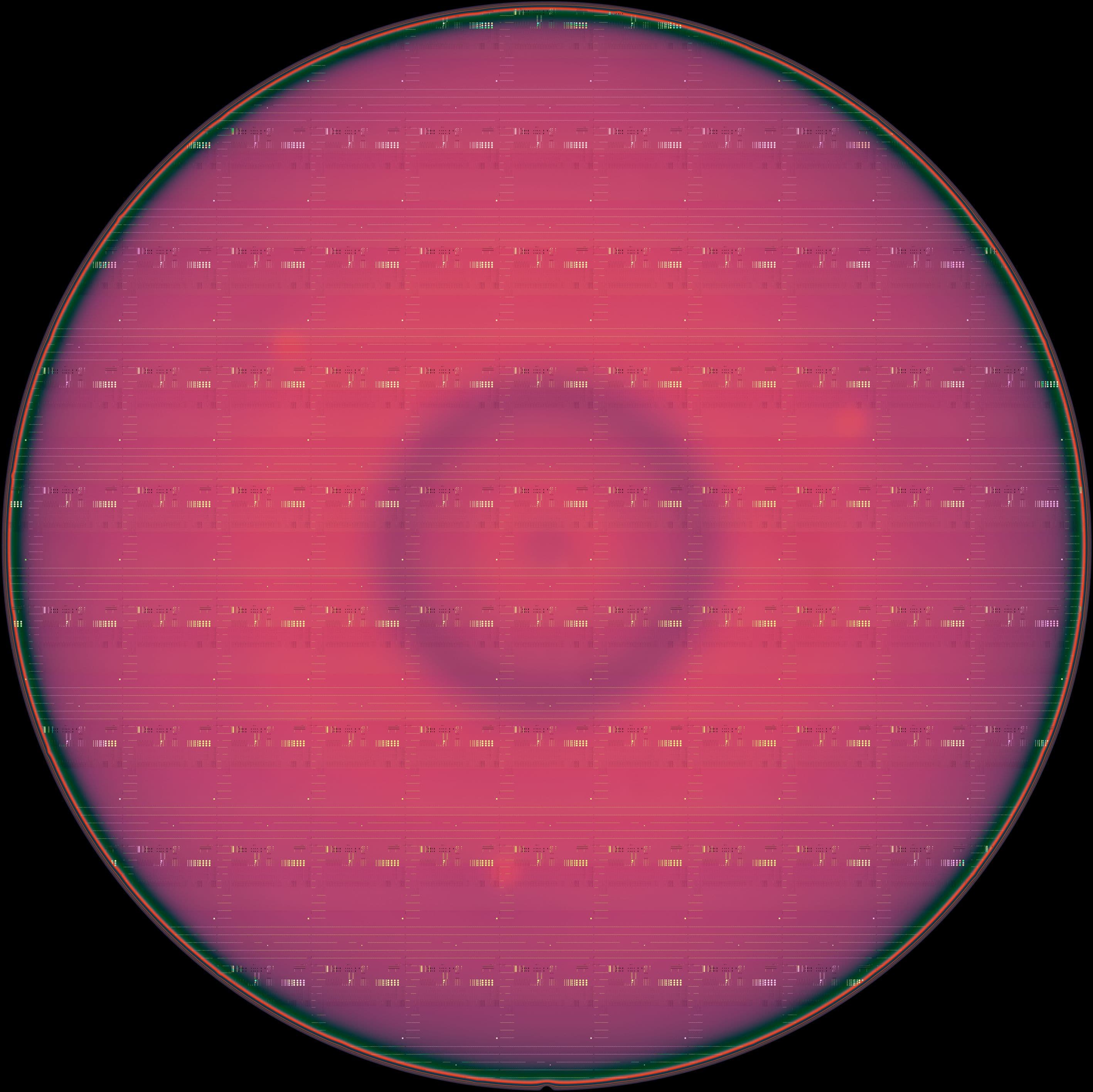
Imec announces the launch of a new program track centered around 300mm GaN technology development for low and high voltage power electronics applications.
Transitioning to 300mm wafer sizes enables the development of more advanced power electronics devices and a reduction of manufacturing costs.
AIXTRON, GlobalFoundries, KLA Corporation, Synopsys, and Veeco are welcomed as first program partners, underlying full ecosystem development.
LEUVEN (Belgium), October 6, 2025— Imec, a world-leading research and innovation hub in nanoelectronics and digital technologies, welcomes AIXTRON, GlobalFoundries, KLA Corporation, Synopsys, and Veeco as first partners in its 300mm gallium-nitride (GaN) open innovation program track for low- and high-voltage power electronics applications. This program track, part of imec’s industrial affiliation program (IIAP) on GaN power electronics, has been set up to develop 300mm GaN epi growth, and low and high voltage GaN high electron mobility transistor (HEMT) process flows. The use of 300mm substrates will not only reduce GaN device manufacturing costs, but it will also allow the development of more advanced power electronics devices, such as efficient low-voltage point-of-load converters for CPUs and GPUs.
The recent market introduction of GaN-based fast battery chargers underscores the potential of GaN technology for power electronics applications. Backed by continuing progress made in GaN epi growth, GaN device and IC manufacturing, reliability and robustness, and system-level optimization, GaN technology is poised to enable a new generation of power electronics products.
These will enter the market with reduced form factors, smaller weight, and superior energy conversion efficiency compared to Si-based solutions. Examples are on-board chargers and DC/DC converters for automotive applications, inverters for solar panels, and power distribution systems for telecom and AI data centers – where GaN-based building blocks contribute to the overall decarbonization, electrification and digitalization of society.
A notable trend in GaN technology development is the move to larger wafer diameters, with capacity now mostly available on 200mm. With the launch of its 300mm GaN program track, imec is taking the next step, building on its 200mm expertise.
Stefaan Decoutere, fellow and program director of the GaN power electronics program at imec: “The benefits of transitioning to 300mm wafers go beyond upscaling production and reducing manufacturing costs. Our CMOS-compatible GaN technology now has access to 300mm state-of-the-art equipment that will allow us to develop more advanced GaN-based power devices. Examples are aggressively scaled low-voltage p-GaN gate HEMTs for use in point-of-load converters, supporting energy-efficient power distribution for CPUs and GPUs.”
As part of the 300mm GaN program, a baseline lateral p-GaN HEMT technology platform will first be established for low-voltage applications (100V and beyond), using 300mm Si(111) as a substrate. For this, process module work centered around p-GaN etch and Ohmic contact formation is ongoing. Later, high-voltage applications are targeted. For 650V and above, developments will utilize 300mm semi-spec and CMOS-compatible QST® engineered substrates (a material with poly-crystalline AlN core). During the developments, control over the bow of the 300mm wafers, and their mechanical strength are prime concerns.
The launch of the 300mm GaN program follows successful 300mm wafer handling tests and mask set development. Imec expects to have full 300mm capabilities installed in its 300mm cleanroom by the end of 2025.
“The success of the 300mm GaN development also hinges on the ability to establish a robust ecosystem and jointly drive innovation from 300mm GaN growth and process integration to packaging solutions,” adds Stefaan Decoutere. “We are therefore pleased to announce AIXTRON, GlobalFoundries, KLA Corporation, Synopsys, and Veeco as first partners in our open R&D program track on 300mm GaN and hope to welcome more partners soon. Because developing advanced GaN power electronics requires close coupling between design, epitaxy, process integration, and applications – a coupling that has proved to be critical for our pioneering work on 200mm GaN.”
About imec
Imec is a world-leading research and innovation center in nanoelectronics and digital technologies. Imec leverages its state-of-the-art R&D infrastructure and its team of more than 6.000 employees and top researchers, for R&D in advanced semiconductor and system scaling, silicon photonics, artificial intelligence, beyond 5G communications and sensing technologies, and in application domains such as health and life sciences, mobility, industry 4.0, agrofood, smart cities, sustainable energy, education, …
Imec unites world-industry leaders across the semiconductor value chain, Flanders-based and international tech, pharma, medical and ICT companies, start-ups, and academia and knowledge centers. Imec is headquartered in Leuven (Belgium), and has research sites across Belgium, in the Netherlands, the UK and the USA, and representation in 3 continents. In 2024, imec's revenue (P&L) totaled 1,034 billion euro.
Further information on imec can be found at www.imec-int.com.
The imec group holds a global trademark portfolio, including word marks and combined figurative registered and unregistered trademarks, across national, regional, and international territories. Its lawful use requires prior written consent of IMEC in compliance with the IMEC branding guidelines, which may be updated periodically. The latest version is available upon written request.
Discover more




GaN-based devices for advanced RF applications: a technology building block in the spotlight
Read more
Imec demonstrates successful monolithic integration of Schottky diodes and depletion-mode HEMTs with 200 V GaN-IC
Read more