Imec and AIXTRON Demonstrate 200 mm GaN Epitaxy on AIX G5+ C for 1200V Applications with Breakdown in Excess of 1800V
This breakthrough result paves the way for GaN to enter into the SiC high voltage domain

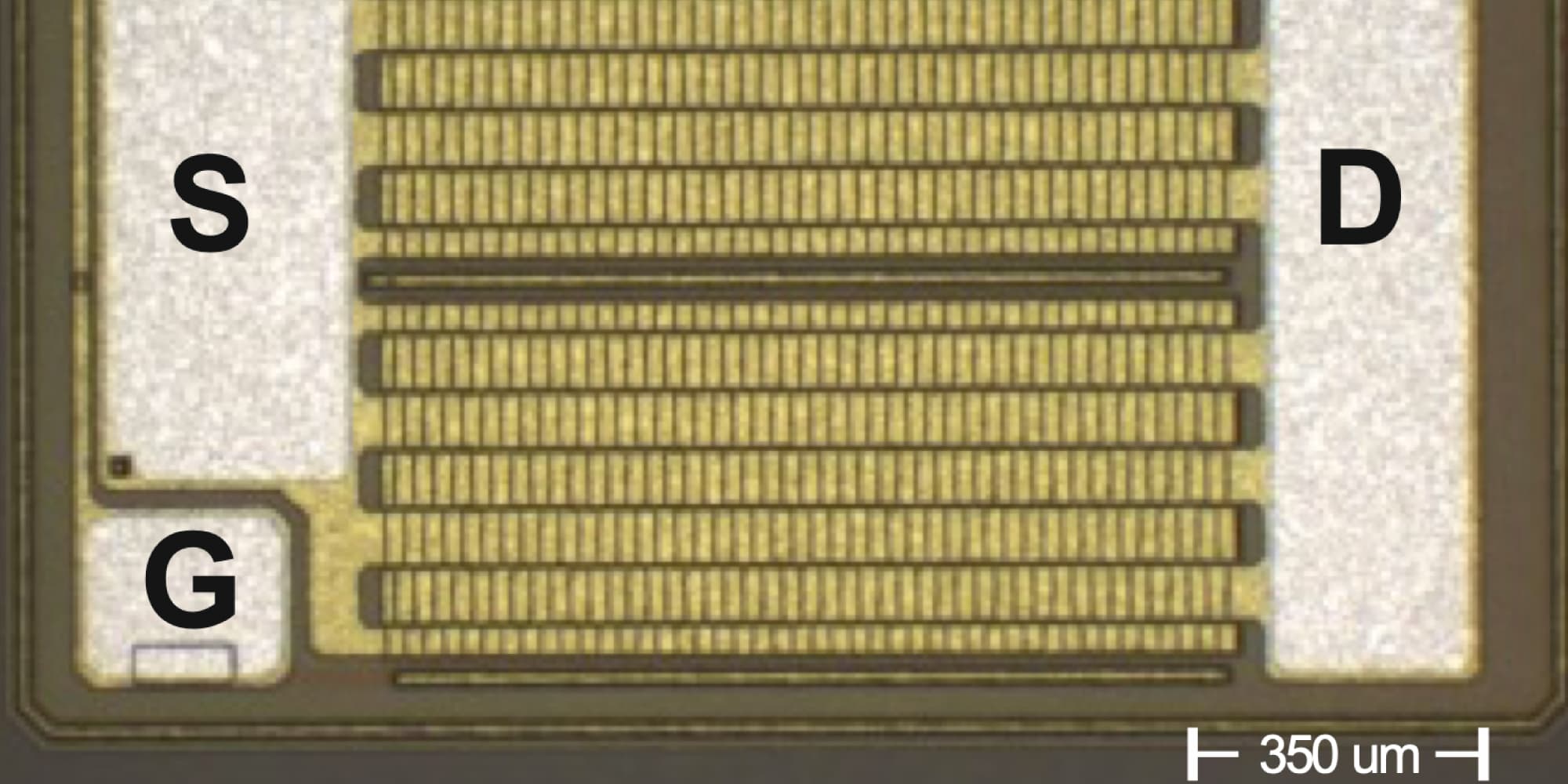
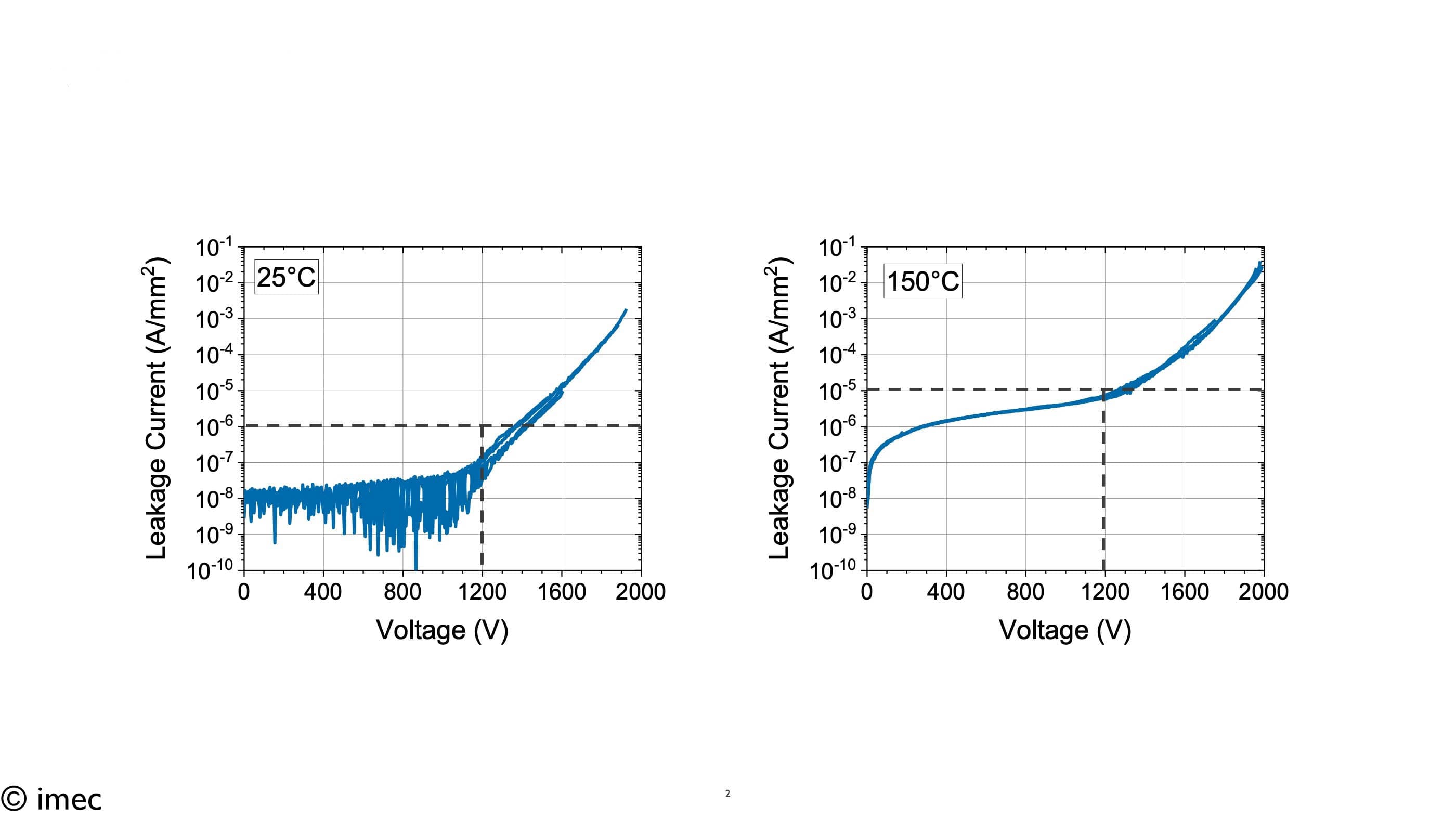
LEUVEN (Belgium), APRIL 29, 2021 — Imec, a world-leading research and innovation hub in nanoelectronics and digital technologies, and AIXTRON, the leading provider of deposition equipment for compound semiconductor materials, have demonstrated epitaxial growth of gallium-nitride (GaN) buffer layers qualified for 1200V applications on 200mm QST® substrates, with a hard breakdown exceeding 1800V. The manufacturability of 1200V-qualified buffer layers opens doors to highest voltage GaN-based power applications such as electric cars, previously only feasible with silicon-carbide (SiC)-based technology. The result comes after the successful qualification of AIXTRON’s G5+ C fully automated metal-organic chemical vapor deposition (MOCVD) reactor at imec, Belgium, for integrating the optimized material epi-stack.
Wide-bandgap materials gallium-nitride (GaN) and silicon-carbide (SiC) have proved their value as next-generation semiconductors for power-demanding applications where silicon (Si) falls short. SiC-based technology is the most mature, but it is also more expensive. Over the years tremendous progress has been made with GaN-based technology grown on for example 200mm Si wafers. At imec, qualified enhancement mode high-electron-mobility transistors (HEMTs) and Schottky diode power devices have been demonstrated for 100V, 200V and 650V operating voltage ranges, paving the way for high-volume manufacturing applications. However, achieving operating voltages higher than 650V has been challenged by the difficulty of growing thick-enough GaN buffer layers on 200mm wafers. Therefore, SiC so far remains the semiconductor of choice for 650-1200V applications – including for example electric cars and renewable energy.
For the first time, imec and AIXTRON have demonstrated epitaxial growth of GaN buffer layers qualified for 1200V applications on 200mm QST® (in SEMI standard thickness) substrates at 25°C and 150°C, with a hard breakdown exceeding 1800V. Denis Marcon, Senior Business Development Manager at imec: “GaN can now become the technology of choice for a whole range of operating voltages from 20V to 1200V. Being processable on larger wafers in high-throughput CMOS fabs, power technology based on GaN offers a significant cost advantage compared to the intrinsically expensive SiC-based technology.”
Key to achieving the high breakdown voltage is the careful engineering of the complex epitaxial material stack in combination with the use of 200mm QST® substrates, executed in scope of the IIAP program The CMOS-fab friendly QST® substrates from Qromis have a thermal expansion that closely matches the thermal expansion of the GaN/AlGaN epitaxial layers, paving the way for thicker buffer layers – and hence higher voltage operation.
Dr. Felix Grawert, CEO and President of AIXTRON “The successful development of imec’s 1200V GaN-on-QST® epi-technology into AIXTRON’s MOCVD reactor is a next step in our collaboration with imec. Earlier, after having installed AIXTRON G5+C at imec’s facilities, imec’s proprietary 200mm GaN-on-Si materials technology was qualified on our G5+ C high-volume manufacturing platform, targeting for example high-voltage power switching and RF applications and enabling our customer to achieve a rapid production ramp-up by pre-validated available epi-recipes. With this new achievement, we will be able to jointly tap into new markets.” Currently, lateral e-mode devices are being processed to prove device performance at 1200V, and efforts are ongoing to extend the technology towards even higher voltage applications. Next to this, imec is also exploring 8-inch GaN-on-QST® vertical GaN devices to further extend the voltage and current range of GaN-based technology.
Results incorporated in this standard received funding from the ECSEL Joint Undertaking (JU) under grant agreement No 783174 (HiPERFORM). The JU receives support from the European Union’s Horizon 2020 research and innovation programme and Austria, Spain, Belgium, Germany, Slovakia, Italy, Netherlands, Slovenia.
About imec
Imec is a world-leading research and innovation hub in nanoelectronics and digital technologies. The combination of our widely acclaimed leadership in microchip technology and profound software and ICT expertise is what makes us unique. By leveraging our world-class infrastructure and local and global ecosystem of partners across a multitude of industries, we create groundbreaking innovation in application domains such as healthcare, smart cities and mobility, logistics and manufacturing, energy and education.
As a trusted partner for companies, start-ups and universities we bring together more than 4,000 brilliant minds from almost 100 nationalities. Imec is headquartered in Leuven, Belgium and has distributed R&D groups at a number of Flemish universities, in the Netherlands, Taiwan, USA, and offices in China, India and Japan. In 2019, imec's revenue (P&L) totaled 640 million euro.
Further information on imec can be found at www.imec-int.com.
Imec is a registered trademark for the activities of imec International (IMEC International, a legal entity set up under Belgian law as a “stichting van openbaar nut”), imec Belgium (IMEC vzw supported by the Flemish Government), imec the Netherlands (Stichting IMEC Nederland, imec Taiwan (IMEC Taiwan Co.), imec China (IMEC Microelectronics (Shanghai) Co. Ltd.), imec India (IMEC India Private Limited), imec San Francisco (IMEC Inc.) and imec Florida (IMEC USA Nanoelectronics Design Center Inc.).
Discover more


Imec launches 300mm GaN program to develop advanced power devices and reduce manufacturing costs
Read more

GaN-based devices for advanced RF applications: a technology building block in the spotlight
Read more