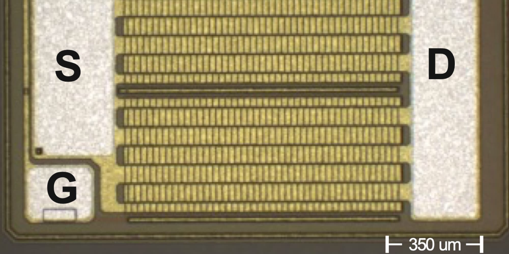
Imec demonstrates successful monolithic integration of Schottky diodes and depletion-mode HEMTs with 200 V GaN-IC
The addition of these components will boost the performance of GaN power systems.
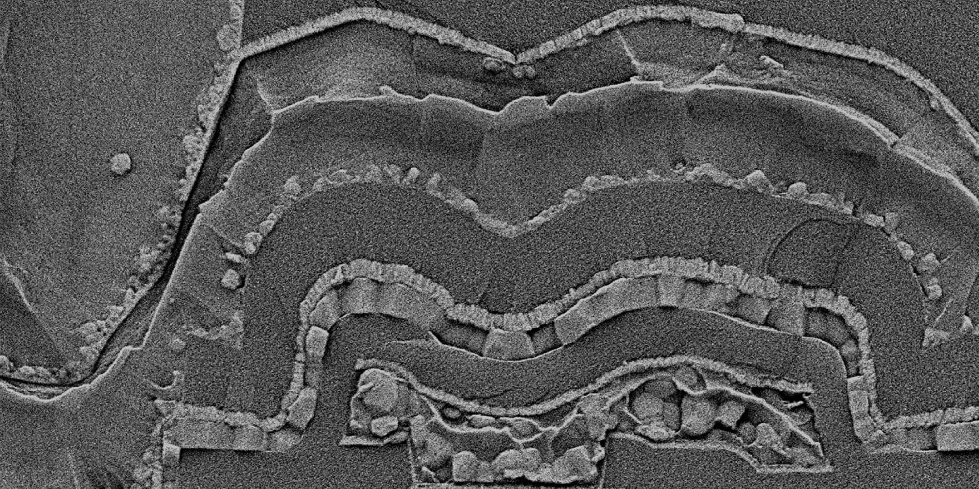
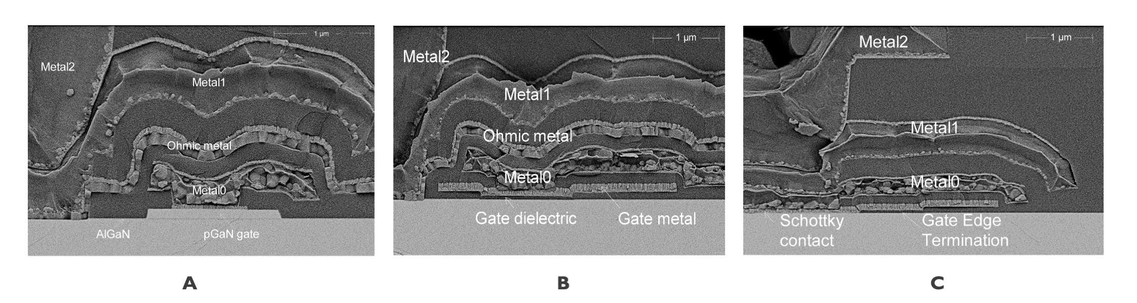
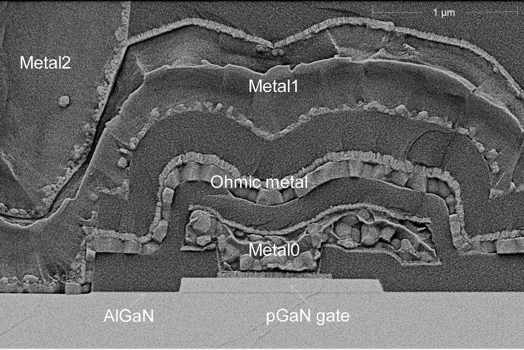
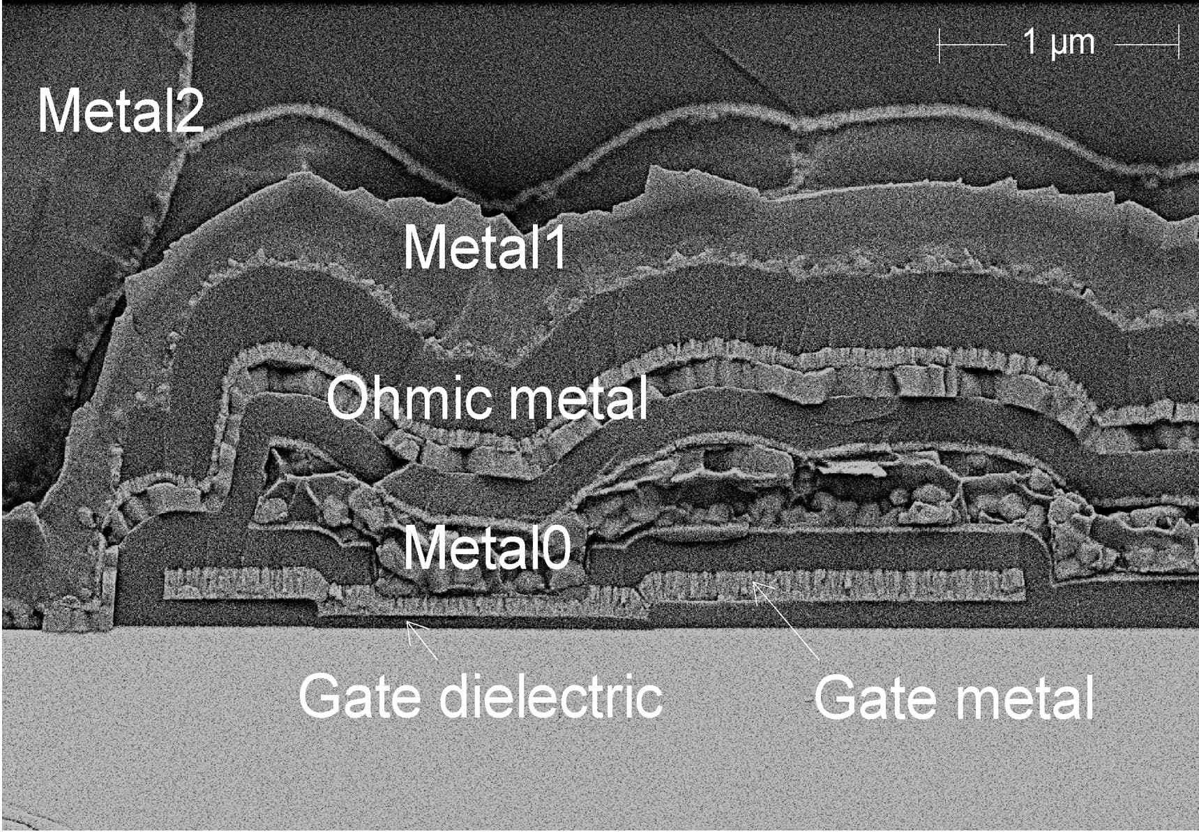
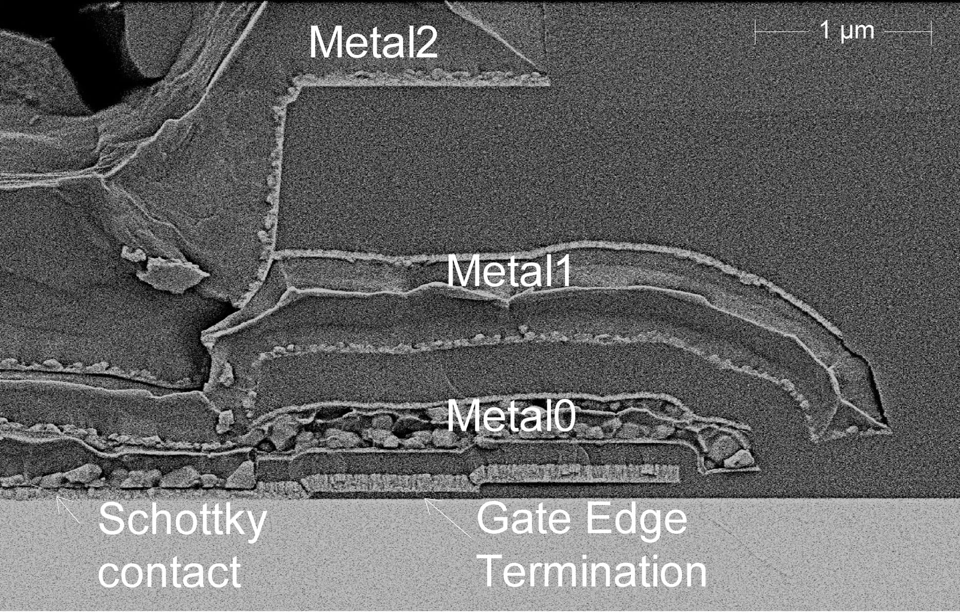
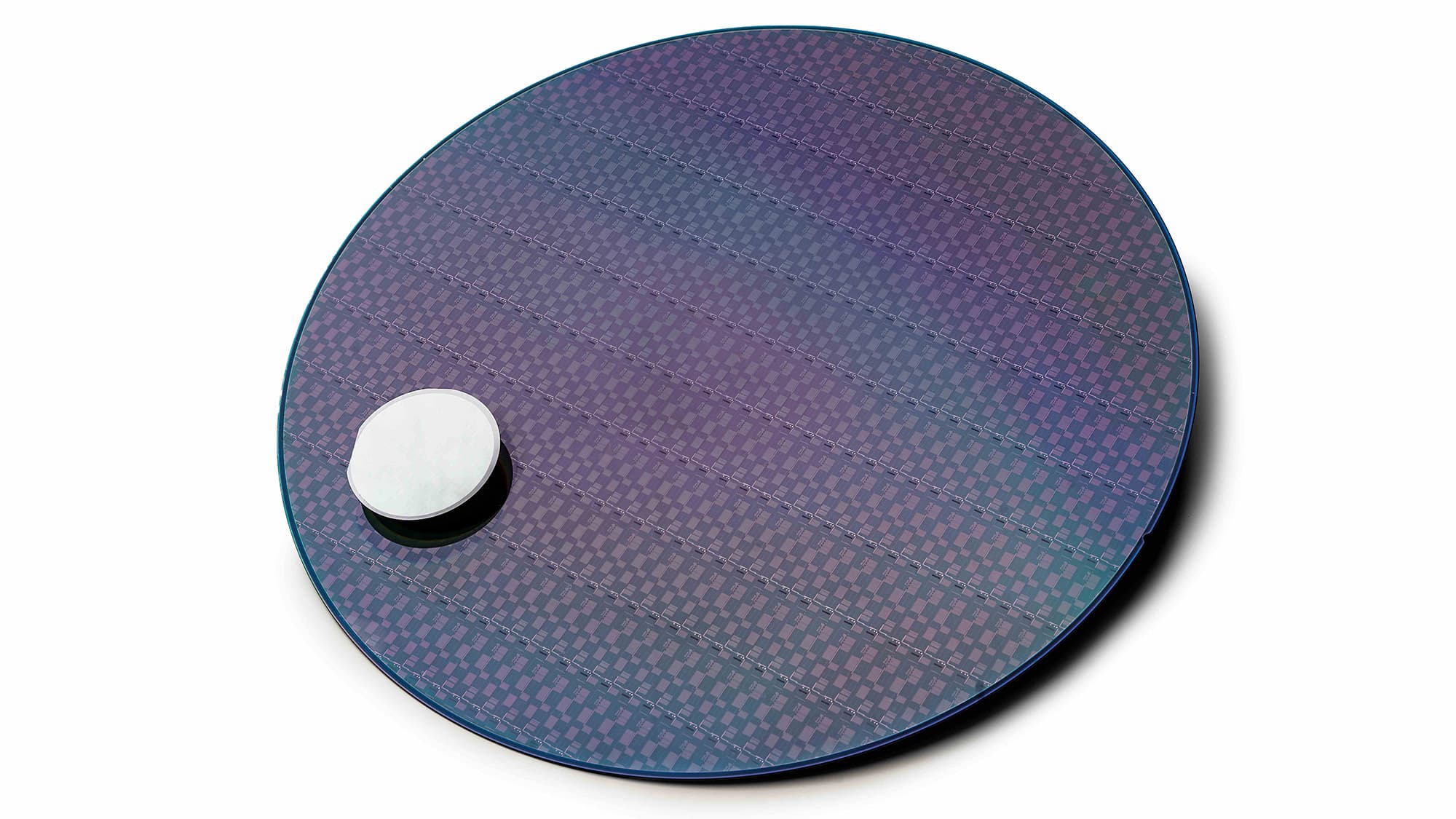
LEUVEN (Belgium), 13 December 2021—This week, at the 2021 International Electron Devices Meeting (IEEE IEDM 2021), imec, a world-leading research and innovation center in nanoelectronics and digital technologies, presents the successful co-integration of high-performance Schottky barrier diodes and depletion-mode HEMTs on a p-GaN HEMT-based 200 V GaN-on-SOI smart power integrated circuits (ICs) platform developed on 200 mm substrates. The addition of these components enables the design of chips with extended functionality and increases performance that takes monolithically-integrated GaN power ICs one step further. This achievement paves the way towards smaller and more efficient DC/DC convertors and Point-of-Load convertors .
Today, GaN power electronics are still dominated by discrete components driven by an external driver IC that generates the switching signals. However, to take full advantage of the fast-switching speed, GaN offers, monolithic integration of power devices and driver functions is recommended. Imec has already successfully demonstrated the monolithic co-integration of a half-bridge and drivers with control and protection circuits that are key to an integrated all-GaN power IC in one chip.
One of the main hurdles to boost the full performance of GaN power ICs remains finding a suitable solution for the lack of p-channel devices in GaN with acceptable performance. CMOS technology uses complementary and more symmetrical pairs of p- and n-type field-effect transistors (FETs), based on the mobilities of holes and electrons for both types of FETs. However, in GaN, the mobility of holes is about 60 times worse than that of electrons. That means a p-channel device, where holes are the principal carriers, would be 60 times larger than the n-channel counterpart and highly inefficient. A widespread alternative is replacing the P-MOS with a resistor. Resistor-Transistor Logic (RTL) has been employed for GaN ICs but shows trade-offs between switching time and power consumption.
“We have improved the performance of GaN ICs by using a combination of enhancement-mode and depletion-mode switches, called e-mode and d-mode HEMTS. By extending our functional e-mode HEMT platform on SOI with co-integrated d-mode HEMTS, now we can take the step from RTL to direct-coupled FET logic, which is expected to improve speed and reduce the power dissipation of the circuits,” said Stefaan Decoutere, program director of GaN power systems at imec.
Another critical component for co-integration on GaN power ICs is a Schottky barrier diode. GaN Schottky diodes combine higher blocking voltages with reduced switching losses compared to their silicon counterparts.
“We have successfully extended our 200 V GaN-on-SOI e-mode HEMT GaN ICs platform with monolithically-integrated high-performance Schottky barrier diodes and d-mode HEMTs, which brings us a step closer to smart power ICs based on GaN. This GaN-IC platform is available for prototyping through our multi-project-wafer (MPW) service,” adds Stefaan Decoutere. “Our platform is ready for transfer to partners. We’re looking for foundries, but also design houses and end-users. The next step will be developing and releasing a 650 Volt version of the platform. Target applications for GaN-on-SOI technology include high-voltage power switching and power conversion, fast chargers for mobile phones, tablets and laptops, and on-board chargers for electric cars, and invertors for solar panel connections to the grid”.
About imec
Imec is a world-leading research and innovation center in nanoelectronics and digital technologies. Imec leverages its state-of-the-art R&D infrastructure and its team of more than 5,000 employees and top researchers, for R&D in advanced semiconductor and system scaling, silicon photonics, artificial intelligence, beyond 5G communications and sensing technologies, and in application domains such as health and life sciences, mobility, industry 4.0, agrofood, smart cities, sustainable energy, education, … Imec unites world-industry leaders across the semiconductor value chain, Flanders-based and international tech, pharma, medical and ICT companies, start-ups, and academia and knowledge centers. Imec is headquartered in Leuven (Belgium) and has research sites across Belgium, the Netherlands, the USA, and offices in India, Taiwan, and Japan. In 2020, imec's revenue (P&L) totaled 680 million euro.
Further information on imec can be found at www.imec-int.com.
Imec is a registered trademark for the activities of imec International (IMEC International, a legal entity set up under Belgian law as a “stichting van openbaar nut”), imec Belgium (IMEC vzw supported by the Flemish Government), imec the Netherlands (Stichting IMEC Nederland), imec Taiwan (IMEC Taiwan Co.), imec India (IMEC India Private Limited), imec San Francisco (IMEC Inc.) and imec Florida (IMEC USA Nanoelectronics Design Center Inc.).
Discover more


Imec launches 300mm GaN program to develop advanced power devices and reduce manufacturing costs
Read more

GaN-based devices for advanced RF applications: a technology building block in the spotlight
Read more