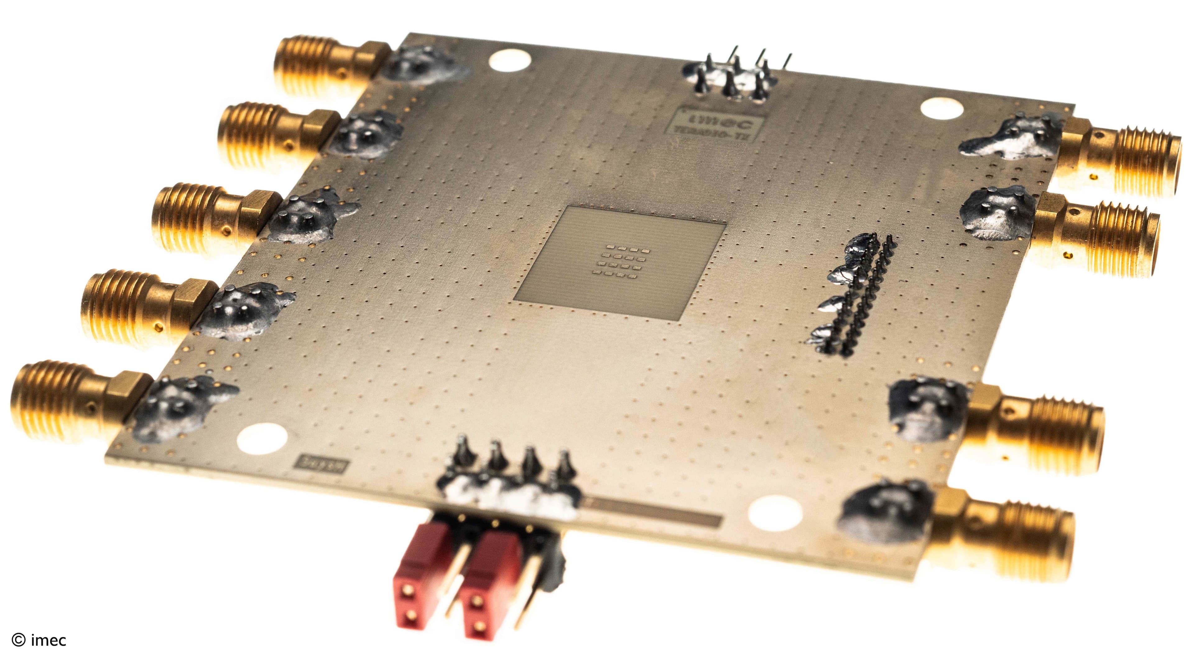
GaN-based devices for advanced RF applications: a technology building block in the spotlight
Study unveils the mechanism behind ion implantation isolation of GaN HEMTs.

In short
Gallium-nitride (GaN) based devices integrated with GaN-on-silicon (GaN-on-Si) technology are expected to play an important role in RF/lower mmWave mobile communication.
Optimizing the devices for this application requires several technology innovations, which may be backed by a better understanding of the physics behind their operation.
In this article, Hao Yu, a researcher at imec, and Bertrand Parvais, a principal member of technical staff at imec, shed light on one of the process steps in the integration flow of GaN high-electron-mobility transistors (HEMTs): the technique of ion implantation used to isolate neighboring GaN HEMTs electrically.
With their study, the authors illustrate the significance of modeling activities to complement technology development for taking GaN-based devices to a higher level of maturity.
The potential of GaN HEMTs for mmWave mobile communication
As the demand for bandwidth continues to grow and existing radio spectrum bands get congested, the telecom industry is looking for novel technologies to meet the requirements for future mobile communication. The quest for more bandwidth is inextricably linked with the use of higher radio frequencies and higher operating frequencies mean more available bandwidth. While researchers examine new III-V materials such as indium phosphide for frequencies above 100GHz, they expect GaN-based technology to play a significant role in the lower mmWave part (i.e., below 50GHz) of the RF spectrum. Because of this, GaN is expected to serve the next generation of 5G networks and possibly, early versions of 6G.
GaN advantages
GaN technology owes its potential for RF/lower mmWave communication to its outstanding physical properties: it has high current density, high electron mobility and high breakdown voltage. The technology can handle switching frequencies higher than today’s Si-based technology because of its high mobility. Beyond speed, GaN-based technology is touted for its power handling capabilities, which make it capable of delivering high output power with good energy efficiency. These features can make GaN an attractive technology to use in the power amplifiers (PAs) that reside in the front-end modules of next-generation mobile handsets and small cells. These front-end modules send the RF signals to and from the antennas. The higher power handling capabilities of GaN compared to conventional Si- or SiGe-based technologies translate into a higher transmission range and/or into a smaller number of elements needed to drive the antennas.
Reducing form factor and cost: towards a viable GaN-on-Si technology platform
To be suitable as a PA in user equipment and small cells, the cost and form factor of the device can become as important as its electrical properties. As stated before, GaN helps reduce the form factor of the front-end module thanks to the inherent properties of the technology. But achieving highly scaled form factors requires integrating the miscellaneous components of the RF front-end technology. To help achieve this goal, imec is tuning its GaN-on-Si technology platform towards RF applications, as part of its Advanced RF program.
Imec has selected GaN-on-Si rather than GaN-on-SiC for cost-saving reasons: not only are Si substrates cheaper, but the CMOS-compatible process also enables large-scale manufacturability. GaN-on-Si technology was initially developed for power electronics applications and envisioned to enable power conversion within battery chargers, computers, servers, automotive, lighting systems and photovoltaics. However, several technology innovations are required to make GaN-on-Si suitable for mobile RF applications. Parasitics within the device structures must be suppressed as much as possible to reach high frequencies. Examples of these efforts include reducing the source access resistance with methods like developing technology modules with raised source/drains and reducing gate-related parasitic capacitances. Optimizing the device for higher operating frequencies will also require a further downscaling of the gate length. This benefits a higher fT and fmax, which is a measure of the intrinsic speed of the device. Furthermore, the buffer layer must be made RF-compatible to minimize the RF substrate losses.
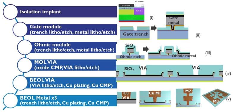
Imec’s GaN-on-Si process flow for RF starts with the metal-organic chemical vapor deposition growth of an epitaxial structure on 200 mm Si wafers. The epitaxial structure is comprised of a proprietary GaN/AlGaN buffer structure, a GaN channel, an AlN spacer and an AlGaN barrier. GaN HEMT devices with TiN Schottky metal gate are subsequently integrated with a low temperature three-level Cu back-end-of-line process as shown in Figure 1.
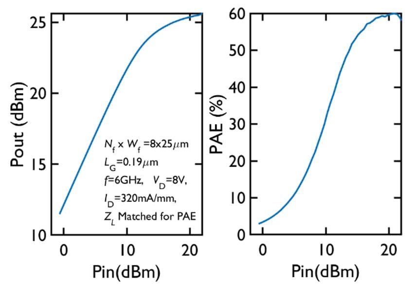
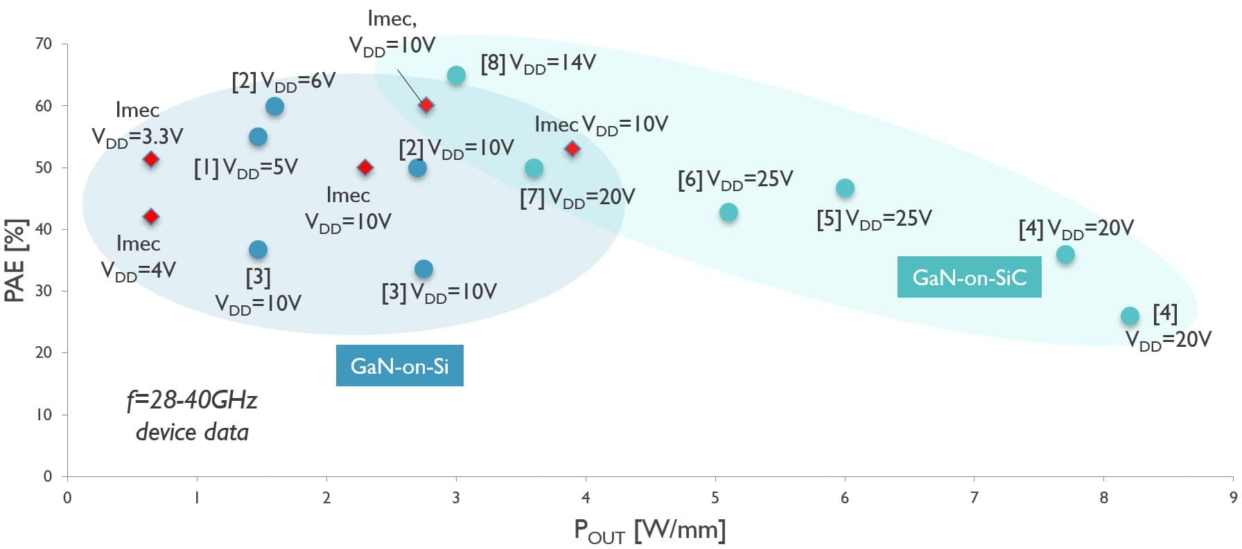
Imec researchers used this CMOS-compatible platform to fabricate GaN HEMTs, as demonstrated at the 2020 International Electron Devices Meeting (IEDM 2020). Optimizations of the gate metal stack, contact resistance and gate length scaling up to 110nm resulted in devices with an fmax of 135GHz, which represents a step forward towards mmWave applications. Key figures of merit for PAs are the output power and the efficiency that the transistors can deliver. Competitive results are obtained on imec’s GaN-on-Si platform, reaching a power-added efficiency (PAE) of 60 percent and a saturated power output (PSAT) of 2W/mm for an 0.19μm gate length (LG) device at 6GHz. These results, presented at European Microwave Week 2022, are shown in Figure 2a. Figure 2b, presented at IEDM 2022, benchmarks the performance of the imec GaN-on-Si process versus other GaN-on-Si and GaN-on-SiC processes. The imec data in red is among the best reported for GaN-on-Si devices and comparable to GaN-on-SiC devices. Using shorter gate lengths improves the measured performance at 28GHz. With these improvements, imec believes that the PAE of amplifiers designed to meet user equipment requirements and fabricated with a GaN-on-Si process achieve parity with equivalent GaN-on-SiC amplifiers for the first time.
Driven by the growth of the power electronics market in recent years, GaN-on-Si technology has become quite mature, mainly due to the development of technology that was initially intended for power electronics applications. Given the level of maturity, digging into the physics behind device operation provides an additional tool to improve the device characteristics. Imec complements technology development with modeling activities that will ultimately help achieve better performance and reliability. The insights gained will not only benefit the development of GaN HEMT devices for mmWave applications, but they will also enable performance improvements in other application domains, including GaN-based power electronics.
Device isolation by ion implantation
As an example of these modeling activities, this section focuses on device isolation. This is one of the technology building blocks of the GaN-on-Si platform. When integrating GaN HEMTs in a common Si platform, the devices must be electrically isolated from each other, with as few leakage paths as possible between neighboring devices. This electrical isolation reduces power loss and improves the breakdown behavior of active devices. For GaN HEMTs, the ion implantation technique has already proven to be an attractive isolation approach over other isolation techniques, such as mesa etching, providing lower leakage and higher breakdown voltage of the isolation regions. The technique was initially developed for GaN-based power electronics applications, where it is still one of the isolation techniques actively being used today.
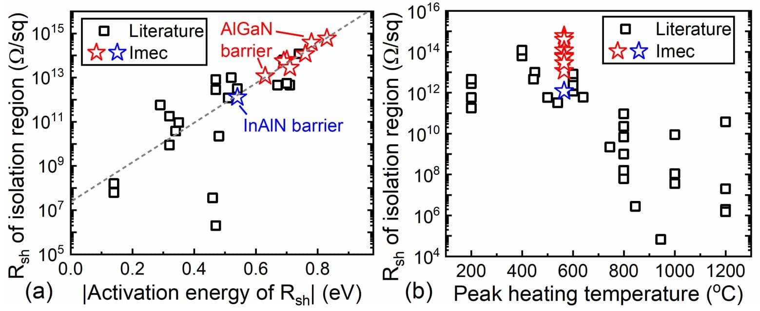
Ion implantation introduces several defects into the GaN heterostructure that act as trapping centers for the charge carriers. In terms of physics, these defects pin the Fermi level away from the conduction or valence band of GaN. Implanting ions, such as nitride (N) ions, in the region surrounding the devices will reduce the number of conductive free carriers, creating an electrically insulating region. In experiments, researchers have also observed that the ion implantation-induced damages disappear after annealing at high temperatures, typically above 600°C, thereby compromising isolation quality. Featuring a low post-epitaxy thermal budget, imec’s GaN-on-Si manufacturing flow guarantees high-quality isolation of HEMT devices. Imec has already demonstrated a GaN HEMT ion implantation isolation technique that contributes to the highest reported sheet resistance, with values in the range of 1013 to 1015Ω/sq. This is an essential metric for quantifying isolation. Figure 3a and Figure 3b illustrates benchmarks of the sheet resistance (Rsh) of AlGaN/(AlN)/GaN heterostructures subjected to ion implantation isolation with varying activation energy magnitudes and peak heating temperatures. The benchmark in Figure 3a suggests a common physical mechanism behind isolation, while the benchmark in Figure 3b indicates the dominant impact of processing temperature on isolation quality.
The mechanism behind ion implantation isolation: a fundamental insight
Why this technique works so well and precisely where the remaining current leakage path is formed has remained a mystery. A fundamental understanding and modeling of the leakage mechanism in ion-implanted regions is needed. This could help improve the process conditions such as thermal budget, implantation dose and energy for various applications, including mmWave communication.
There is a reason why it is so difficult to understand the exact mechanism behind the insulation. The ion-implanted region is full of defects of various natures. There are point defects, such as vacancies or interstitial atoms, defect complexes, foreign ion impurities and lattice disorder to name a few. In addition, polarization charges reside at the interface between AlGaN and GaN. This complex cocktail of defects and charges makes it highly challenging to simulate the behavior of the charges within the isolated heterostructure and to locate the leakage path.
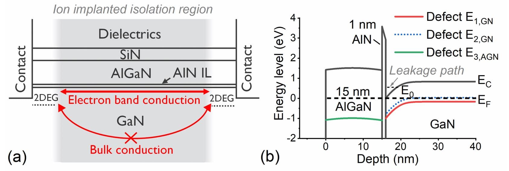
By combining experimental and modeling work, imec researchers have unveiled the leakage mechanism in isolated GaN-based heterostructures for the first time. The details of this work have been published in the Journal of Applied Physics. By setting up dedicated experiments with varying AlGaN and AlN thicknesses, researchers extracted and analyzed the sheet resistances of the isolated regions and the corresponding activation energies. The conclusion from these experiments was that the dominant leakage occurs via an ohmic path of electrons at the GaN surface. Revert to the terms of physics, this translates into a downward bending of the GaN conduction band near the GaN surface. These insights laid the foundation for more detailed modeling of the isolated heterostructure and for reconstructing its energy band diagrams. The theory helped extract the net defect densities in these isolated implanted regions, which amounted to ∼2×1019cm-3 and ∼2×1018cm-3 for GaN and AlGaN, respectively for these experiments. The majority of those defects are found as point defects. The point defects were created by ion implantation techniques and preserved from recombination with imec’s low thermal budget HEMT fabrication. The high densities of point defects are essential to limit the GaN surface energy band bending and thus limit the leakage. Figure 4a and Figure 4b illustrate the leakage mechanism in GaN heterostructures. Figure 4a shows the surface leakage path versus bulk leakage path in transmission line model structures. Figure 4b illustrates the energy band diagram of the AlGaN/AlN/GaN heterostructure showing band bending at the GaN surface.
Conclusion
For the first time, imec researchers have unveiled the exact mechanism behind ion implantation as a technique for electrically isolating GaN HEMT devices. These insights help improve the process conditions to obtain good isolation quality when targeting RF/mmWave communication. The findings can be extended to power electronics applications as well. Moreover, the study led to a novel method to estimate the net defect density in isolated GaN-based heterostructures. These activities fit into the broader framework of GaN device optimization for RF applications through both technology and modeling. The efforts and the results illustrate how uncovering the physics secrets behind the technology building blocks can help take these GaN-based devices to the next level of maturity.
This article was originally published in Microwave Journal.
Want to know more?
You can find more details in the article published in J. Appl. Phys. 131, 035701 (2022). Interested in receiving the ‘Leakage mechanism in ion implantation isolated AlGaN/GaN heterostructures’ article by Hao Yu et al.: fill out the contact form.
Authors

Hao Yu
Hao Yu was born in Jinan, China. He received his B.S. and M.S. degrees in Microelectronics and Solid-State Electronics from Fudan University in 2010 and 2013, respectively. He received the China national graduate student scholarship award and Shanghai excellent graduate student award in 2013. Hao Yu is now a PhD candidate affiliated to imec and Katholieke Universiteit Leuven under supervision of Dr. Marc Schaekers, Dr. Nadine Collaert and Prof. Kristin De Meyer. He has been working on metal-semiconductor contact resistances and semiconductor junction characterizations. As high contact resistances become major obstacles that compromise performance of modern CMOS devices, Hao Yu has developed high-accuracy test vehicles and reported multiple contact schemes meeting the 10–9Ωcm2-contact-resistivity industrial target. He has authored and co-authored 17 articles to peer reviewed journals and 16 to international conferences. He received the IEEE electron device society PhD student fellowship award in 2017, the imec PhD student excellence award in 2018, and the China scholarship council award for outstanding self-financed students abroad in 2018. Since September 2018, Hao Yu has joined Dr. Niamh Waldron’s team at imec as a researcher working on IIIV-on-Si RF technologies.

Bertrand Parvais
Bertrand Parvais is a principal member of the technical staff at imec, in charge of RF and mmWave device technologies. He received his electrical engineering and Ph.D. degrees from the Université Catholique de Louvain, Louvain-la-Neuve, Belgium, in 2000 and 2004, respectively. He joined imec as a device engineer, working on the characterization and modeling of transistors in advanced CMOS technologies for analog and RF applications. From 2009 to 2016, he was involved in designing mixed-mode and millimeter-wave CMOS circuits. Since 2016, he has led imec research teams working on transistor compact models and RF transistor technologies. In parallel, he joined the Vrije Universiteit Brussels (VUB) in 2017 as a guest professor.
Discover more


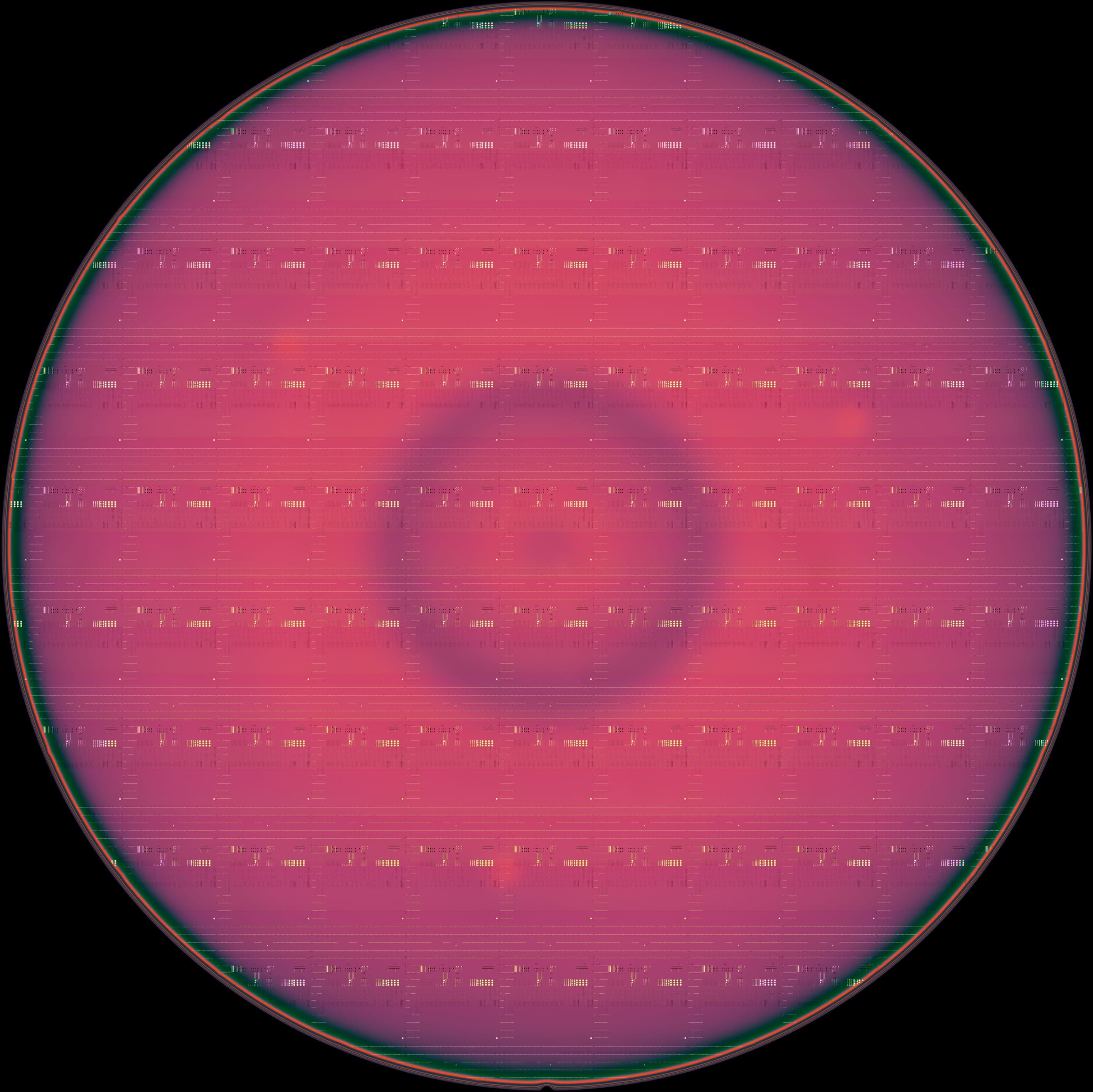
Imec launches 300mm GaN program to develop advanced power devices and reduce manufacturing costs
Read more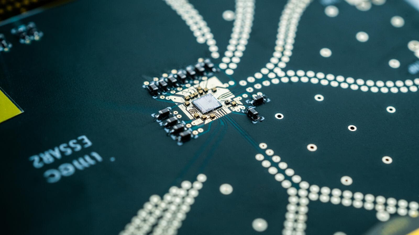
300mm RF silicon interposer platform for chiplet-based heterogeneous integration demonstrates record-low insertion loss at frequencies up to 325GHz
Read more
Disruptive ‘Wi-Fi on steroids’ technology allows manufacturing industry to finally cut the cord
Read more
Imec achieves seamless InP Chiplet integration on 300mm RF Silicon Interposer with excellent performance at 140GHz
Read more