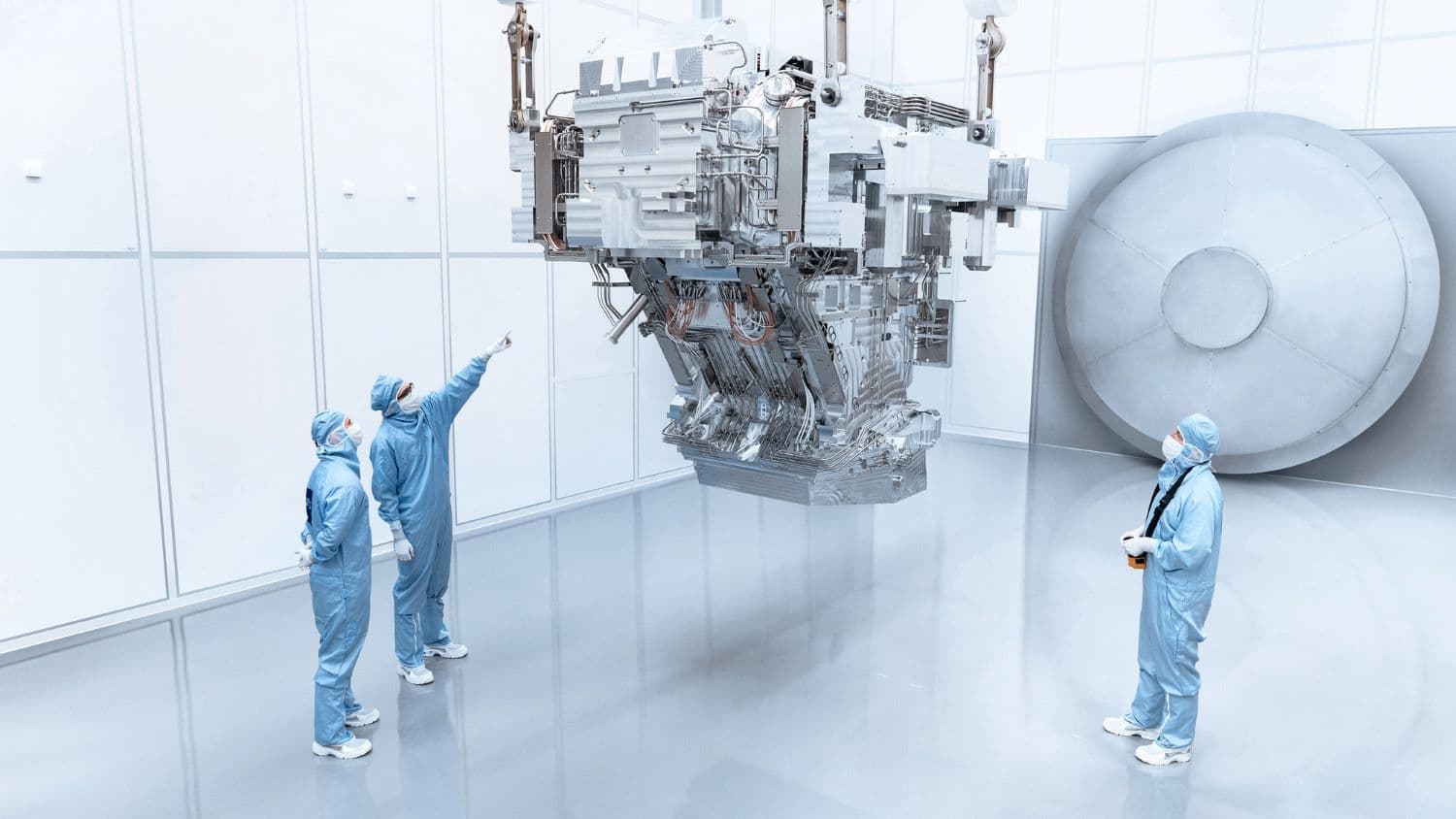
Imec demonstrates logic and DRAM structures using High NA EUV Lithography
Results confirm readiness of the High NA EUV patterning ecosystem for enabling future logic and memory use cases
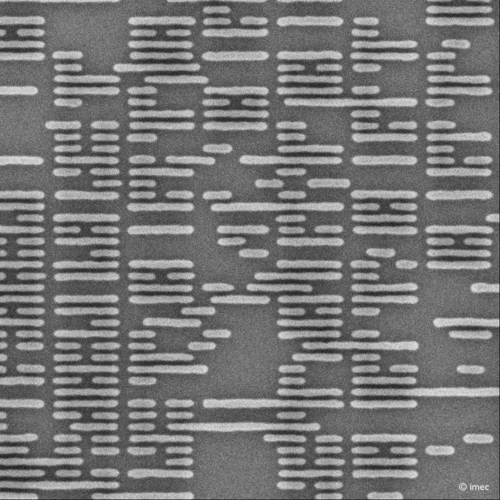
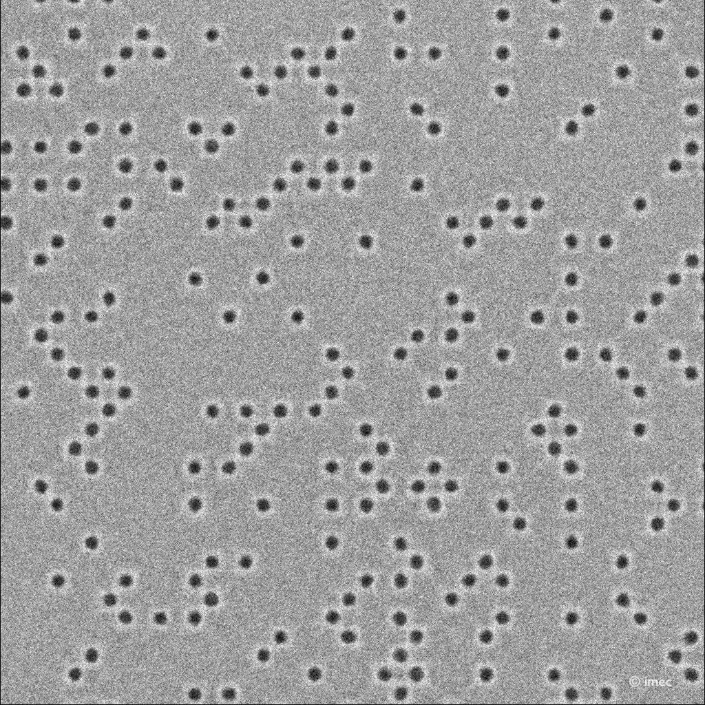
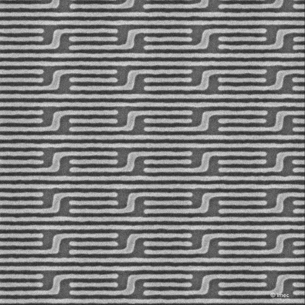
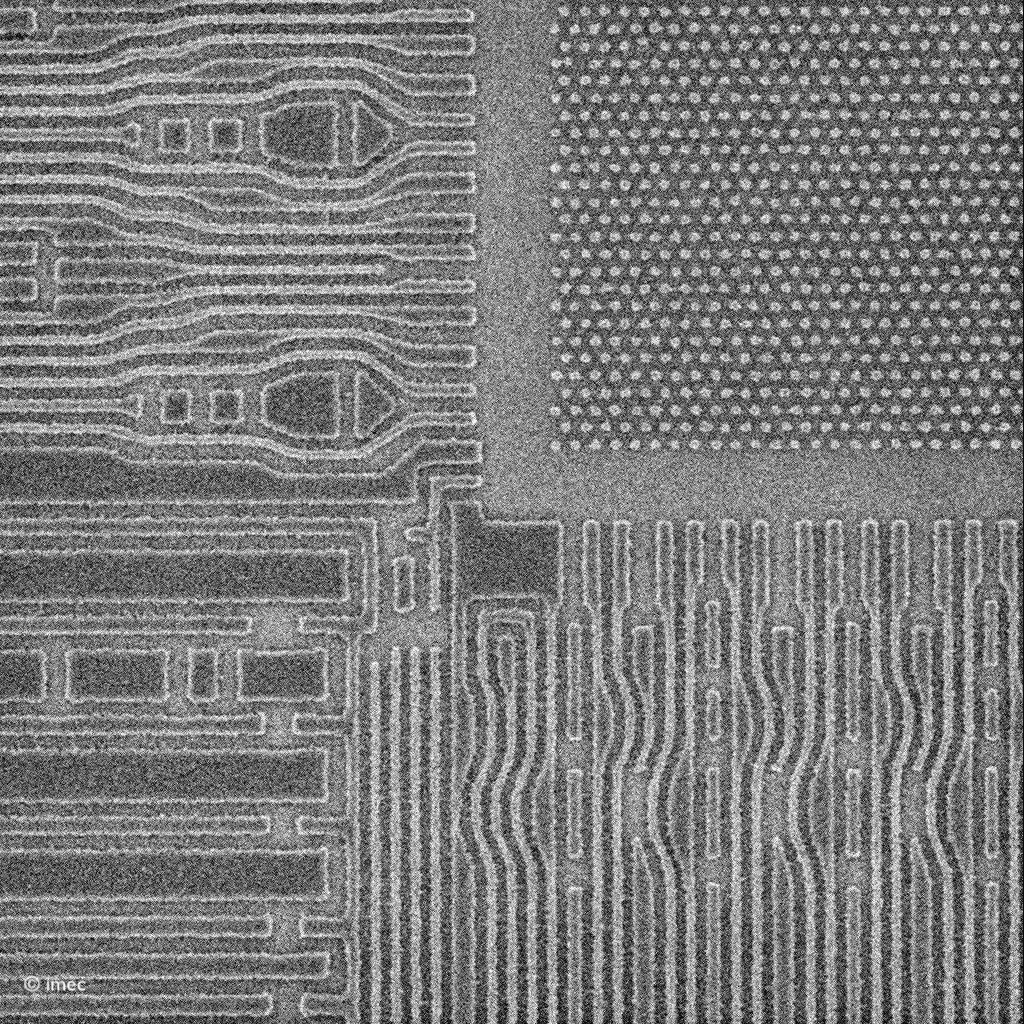
LEUVEN (Belgium), August 7, 2024— Imec, a world-leading research and innovation hub in nanoelectronics and digital technologies, presents patterned structures obtained after exposure with the 0.55NA EUV scanner in the joint ASML-imec High NA EUV Lithography Lab in Veldhoven, the Netherlands. Random logic structures down to 9.5nm (19 nm pitch), random vias with 30nm center-to-center distance, 2D features at 22nm pitch, and a DRAM specific lay out at P32nm were printed after single exposure, using materials and baseline processes that were optimized for High NA EUV by imec and its partners in the framework of imec’s Advanced Patterning Program. With these results, imec confirms the readiness of the ecosystem to enable single exposure high-resolution High NA EUV Lithography.
Following the recent opening of the joint ASML-imec High NA EUV Lithography Lab in Veldhoven, the Netherlands, customers now have access to the (TWINSCAN EXE:5000) High NA EUV scanner to develop private High NA EUV use cases leveraging the customer’s own design rules and lay outs.
Imec has successfully patterned single exposure random logic structures with 9.5nm dense metal lines, corresponding to a 19nm pitch, achieving sub 20nm tip-to-tip dimensions. Random vias with a 30nm center-to-center distance showcased excellent pattern fidelity and critical dimension uniformity. Furthermore, 2D features at a P22nm pitch exhibited outstanding performance, highlighting the potential of High NA Lithography to enable 2D routing.
Beyond logic structures, imec successfully patterned, in a single exposure, designs that integrate the storage node landing pad with the bit line periphery for DRAM. This achievement underscores the potential of High NA technology to replace the need of several mask layers by 1 single exposure.
These breakthrough results follow intensive preparatory work by imec and ASML – in close collaboration with its partners – to ready the patterning ecosystem and metrology for the first generation of High NA EUV Lithography. Prior to the exposures, imec prepared dedicated wafer stacks (including advanced resists, underlayers and photomasks), and transferred High NA EUV baseline processes (such as optical proximity correction (OPC), integrated patterning and etch techniques) to the 0.55NA EUV scanner.
Steven Scheer, senior vice president of compute technologies & systems / compute system scaling at imec: “We are thrilled to demonstrate the world’s first High NA-enabled logic and memory patterning in the joint ASML-imec lab as an initial validation of industry applications. The results showcase the unique potential for High NA EUV to enable single-print imaging of aggressively-scaled 2D features, improving design flexibility as well as reducing patterning cost and complexity. Looking ahead, we expect to provide valuable insights to our patterning ecosystem partners, supporting them in further maturing High NA EUV specific materials and equipment.”
Luc Van den hove, president and CEO of imec: “The results confirm the long-predicted resolution capability of High NA EUV lithography, targeting sub 20nm pitch metal layers in one single exposure. High NA EUV will therefore be highly instrumental to continue the dimensional scaling of logic and memory technologies, one of the key pillars to push the roadmaps deep into the ‘angstrom era'. These early demonstrations were only possible thanks to the set-up of the joint ASML-imec lab allowing our partners to accelerate the introduction of High NA lithography into manufacturing.”.
About imec
Imec is a world-leading research and innovation center in nanoelectronics and digital technologies. Imec leverages its state-of-the-art R&D infrastructure and its team of more than 5,500 employees and top researchers, for R&D in advanced semiconductor and system scaling, silicon photonics, artificial intelligence, beyond 5G communications and sensing technologies, and in application domains such as health and life sciences, mobility, industry 4.0, agrofood, smart cities, sustainable energy, education, … Imec unites world-industry leaders across the semiconductor value chain, Flanders-based and international tech, pharma, medical and ICT companies, start-ups, and academia and knowledge centers. Imec is headquartered in Leuven (Belgium), and has research sites across Belgium, in the Netherlands and the USA, and representation in 3 continents. In 2023, imec's revenue (P&L) totaled 941 million euro.
Further information on imec can be found at www.imec-int.com.
Imec is a registered trademark for the activities of imec International and its affiliated entities.
Discover more

Imec unlocks lever for EUV dose reduction: oxygen injection during metal-oxide resist post-exposure bake emerges as game-changer for throughput
Read more
Imec achieves new milestones in single patterning High NA EUV lithography for both damascene and direct metal etch metallization processes
Read more