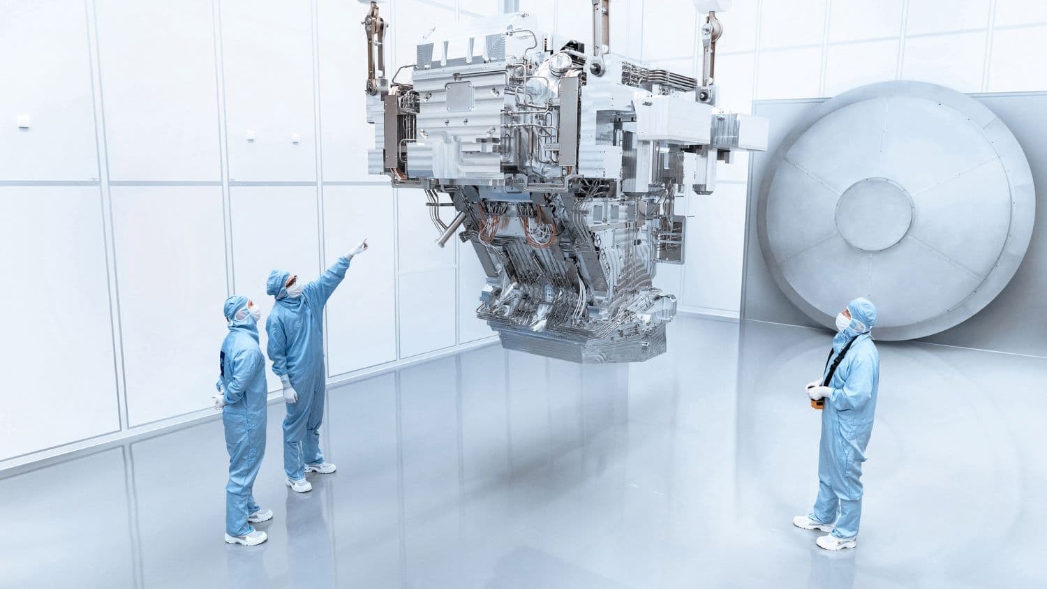
Imec and ASML open joint High NA EUV Lithography Lab offering an early development platform to the leading-edge semiconductor ecosystem
Opening of the joint ASML-imec High NA EUV Lithography Lab marks a milestone in preparing High NA EUV lithography for accelerated adoption in mass manufacturing
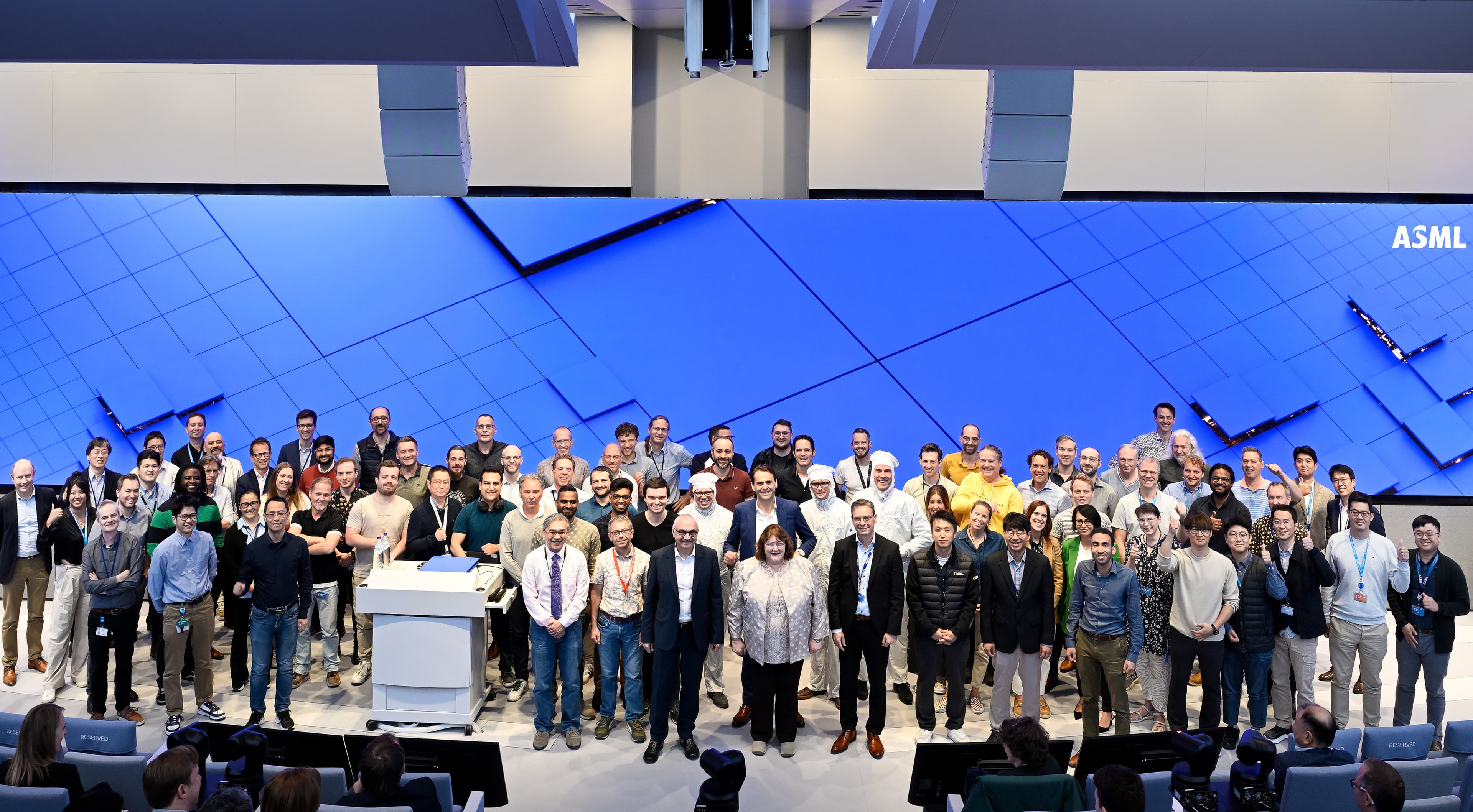
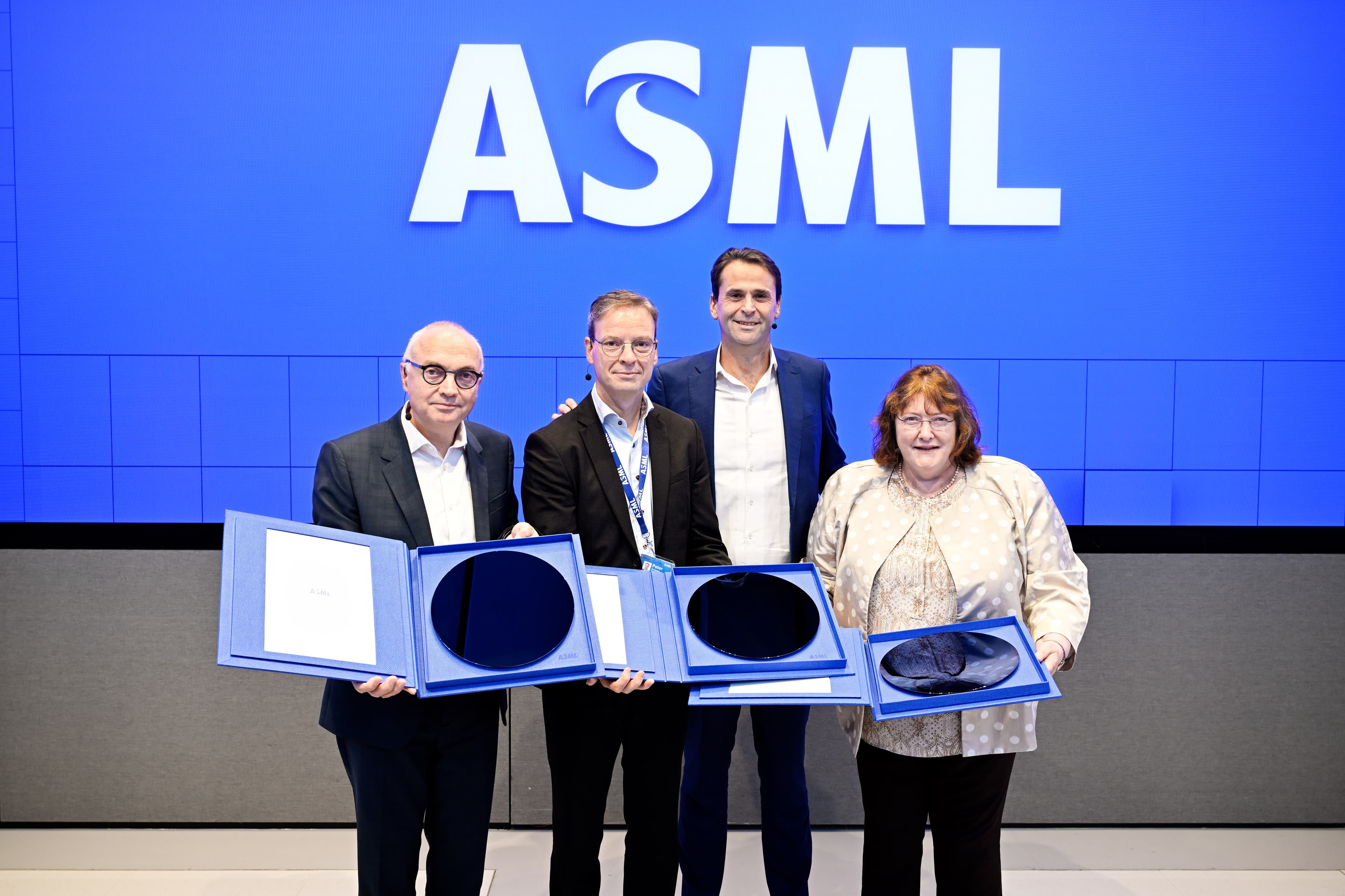
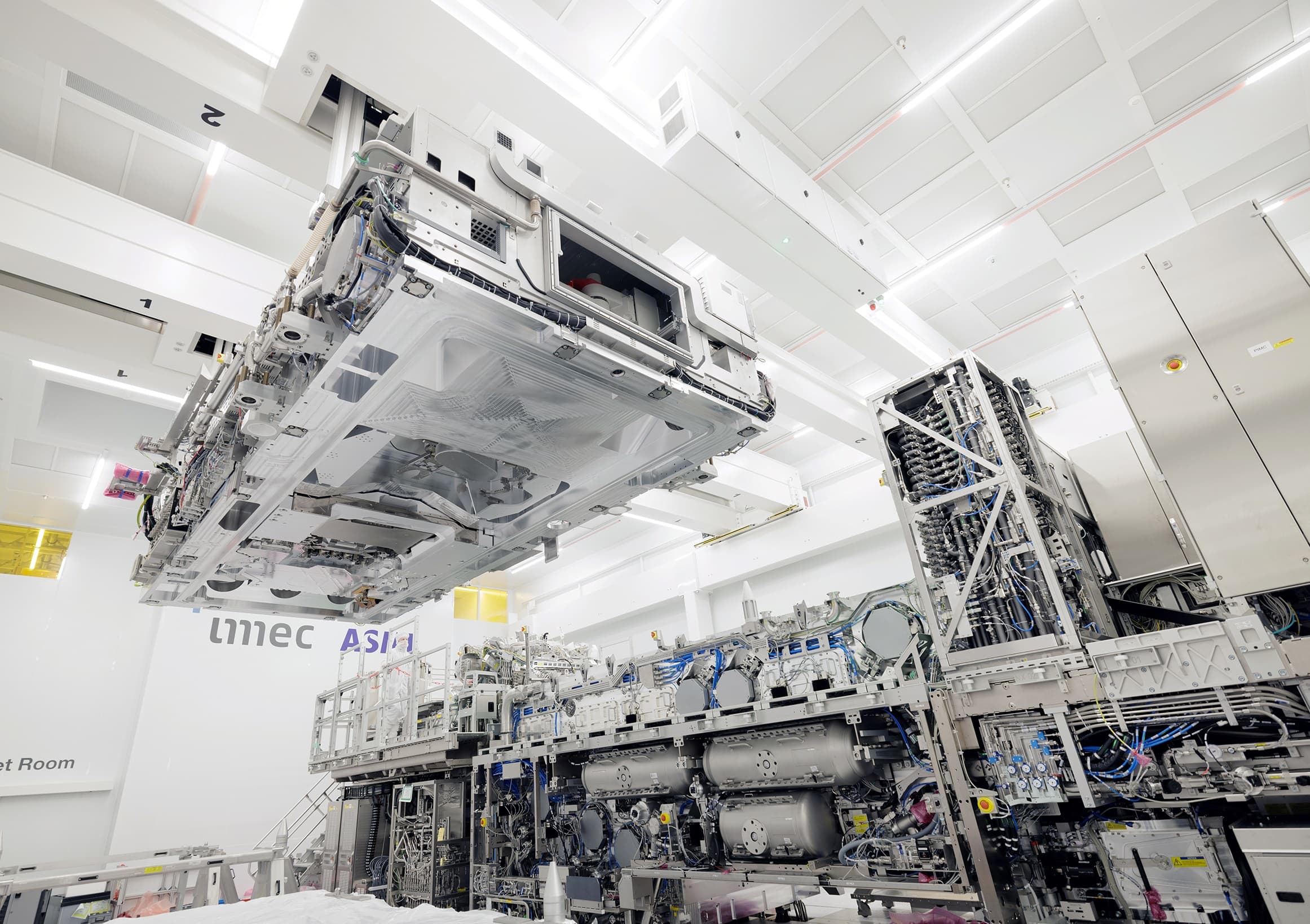
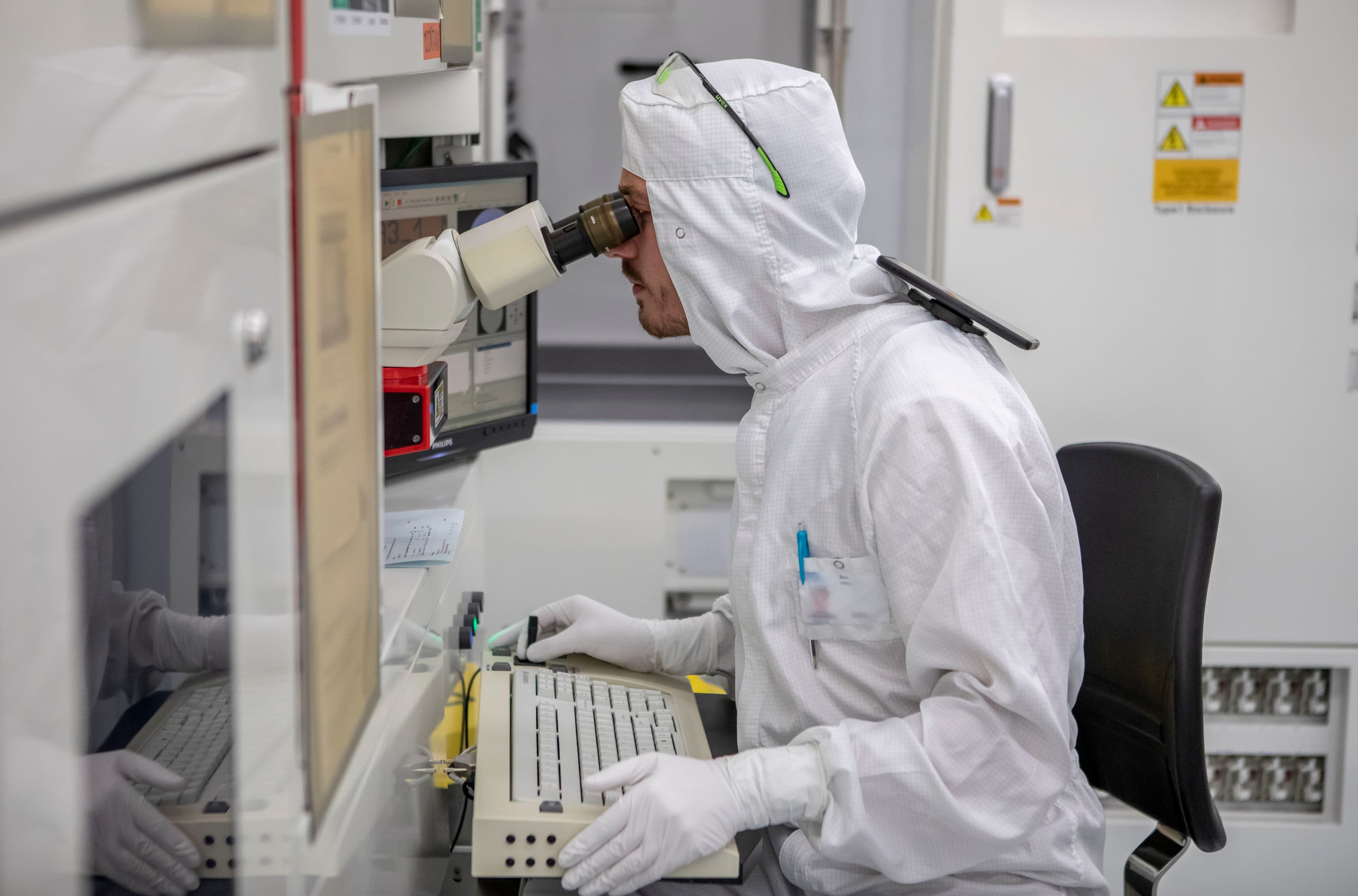
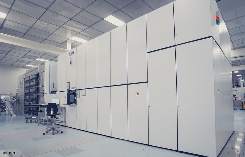
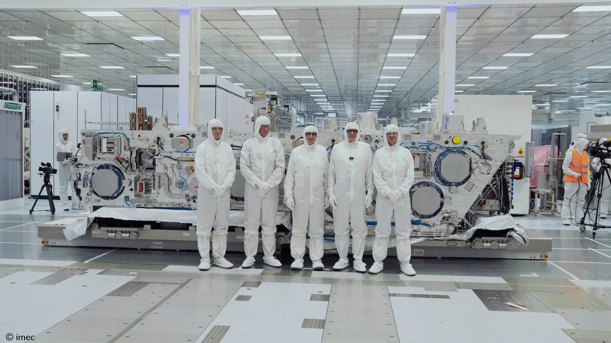
LEUVEN (Belgium) and Veldhoven (the Netherlands), June 3, 2024— Imec, a world-leading research and innovation hub in nanoelectronics and digital technologies, and ASML Holding N.V. (ASML), a leading lithography supplier to the semiconductor industry, today announced the opening of the High NA EUV Lithography Lab in Veldhoven, the Netherlands, a lab jointly run by ASML and imec. After a build and integration period of years, the Lab is ready to provide leading-edge logic and memory chip makers, as well as advanced materials and equipment suppliers access to the first prototype High NA EUV scanner (TWINSCAN EXE:5000) and surrounding processing and metrology tools.
The opening of the joint ASML-imec High NA EUV Lab represents a milestone in preparing High NA EUV for high-volume manufacturing – anticipated to happen in the 2025–2026 timeframe. By giving leading-edge logic and memory chip manufacturers access to the High NA EUV prototype scanner and surrounding tools (which include a coat and development track, metrology tools, wafer and mask handling systems), imec and ASML support them in de-risking the technology and developing private High NA EUV use cases before the scanners will be operational in their production fabs. Access will also be provided to the broader ecosystem of material and equipment suppliers and to imec’s High NA patterning program.
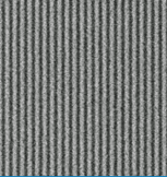
Readying the 0.55 NA EUV scanner and infrastructure followed intense preparations that started in 2018. In this time span, ASML and ZEISS were able to develop High NA EUV scanner-specific solutions related to the source, optics, lens anamorphicity, stitching, reduced depth of focus, edge placement errors and overlay accuracy. Meanwhile, imec, in tight collaboration with its extended supplier network, prepared the patterning ecosystem, including the development of advanced resist and underlayer materials, photomasks, metrology and inspection techniques, (anamorphic) imaging strategies, optical proximity correction (OPC), and integrated patterning and etch techniques. The preparatory work recently resulted in first exposures, showing for the first time ever 10 nm dense lines (20 nm pitch) printed in Veldhoven on metal oxide resists (MORs) using the 0.55 NA EUV prototype scanner.
Imec’s president and CEO Luc Van den hove: “High NA EUV is the next milestone in optical lithography, promising the patterning of metal lines/spaces with 20 nm pitch in one single exposure and enabling next generations of DRAM chips. This will improve yield and reduce cycle time and even CO2 emissions compared to existing multi-patterning 0.33 NA EUV schemes. It will therefore be a key enabler to push Moore’s Law well into the ångström era. We are now thrilled to explore these capabilities in real life, using the prototype High NA EUV scanner. For imec and its partners, the High NA EUV Lithography Lab will act as a virtual extension of our 300 mm cleanroom in Leuven, enabling us to further improve the patterning ecosystem and push the resolution of the High NA EUV towards its ultimate limits.”
ASML’s President and CEO Christophe Fouquet: “The ASML-imec High NA EUV Lithography Lab provides an opportunity for our EUV customers, partners and suppliers to access the High NA EUV system for process development while waiting for their own system to be available at their factories. This type of very early engagement with the ecosystem is unique and could significantly accelerate the learning curve on the technology and smoothen the introduction in manufacturing. We are committed to work with and support our customers in this journey with High NA EUV.”
About imec
Imec is a world-leading research and innovation center in nanoelectronics and digital technologies. Imec leverages its state-of-the-art R&D infrastructure and its team of more than 5,500 employees and top researchers, for R&D in advanced semiconductor and system scaling, silicon photonics, artificial intelligence, beyond 5G communications and sensing technologies, and in application domains such as health and life sciences, mobility, industry 4.0, agrofood, smart cities, sustainable energy, education, … Imec unites world-industry leaders across the semiconductor value chain, Flanders-based and international tech, pharma, medical and ICT companies, start-ups, and academia and knowledge centers. Imec is headquartered in Leuven (Belgium), and has research sites across Belgium, in the Netherlands and the USA, and representation in 3 continents. In 2023, imec's revenue (P&L) totaled 941 million euro.
Further information on imec can be found at www.imec-int.com.
Imec is a registered trademark for the activities of imec International (IMEC International, a legal entity set up under Belgian law as a “stichting van openbaar nut”), imec Belgium (IMEC vzw supported by the Flemish Government), imec the Netherlands (Stichting IMEC Nederland), imec Taiwan (IMEC Taiwan Co.), imec India (IMEC India Private Limited), imec San Francisco (IMEC Inc.) and imec Florida (IMEC USA Nanoelectronics Design Center Inc.).
About ASML
ASML is a leading supplier to the semiconductor industry. The company provides chipmakers with hardware, software and services to mass produce the patterns of integrated circuits (microchips). Together with its partners, ASML drives the advancement of more affordable, more powerful, more energy-efficient microchips. ASML enables groundbreaking technology to solve some of humanity's toughest challenges, such as in healthcare, energy use and conservation, mobility and agriculture. ASML is a multinational company headquartered in Veldhoven, the Netherlands, with offices across EMEA, the US and Asia. Every day, ASML’s more than 42,700 employees (FTE) challenge the status quo and push technology to new limits. ASML is traded on Euronext Amsterdam and NASDAQ under the symbol ASML. Discover ASML – our products, technology and career opportunities – at www.asml.com.
Discover more
Imec unlocks lever for EUV dose reduction: oxygen injection during metal-oxide resist post-exposure bake emerges as game-changer for throughput
Read more
Imec achieves new milestones in single patterning High NA EUV lithography for both damascene and direct metal etch metallization processes
Read more