Scaling CMOS beyond FinFETs: from nanosheets and forksheets to CFETs
The FinFET transistor architecture is the workhorse of today’s semiconductor industry. But as scaling continues, undesired short-channel effects require the introduction of new transistor architectures. In this article, Julien Ryckaert, program director 3D hybrid scaling at imec, sketches out an evolutionary path towards 2nm and beyond technology nodes. Along this exciting road, he introduces the nanosheet transistor, the forksheet device and the CFET. Part of these insights have been presented at the 2019 IEEE International Electron Devices Meeting (IEDM).
The FinFET: today’s leading-edge transistor
At every new technology generation, chipmakers have been able to scale transistor specs by 0.7x, delivering a 15% performance boost, a 50% area gain, a 40% power reduction and a 35% cost decrease at device level. Several years ago, the industry made the transition from ‘good old’ planar MOSFET to FinFET transistor architectures in order to maintain this scaling path. In a FinFET, the channel between source and drain terminals is in the form of a fin. The gate wraps around this 3D channel, providing control from 3 sides of the channel. This multi-gate structure could eliminate short-channel effects, which started to degrade the transistor’s performance at reduced gate lengths.
Superior short-channel control is crucial since it sets the foundations of device scaling – allowing shorter channel lengths and lower operating voltages.
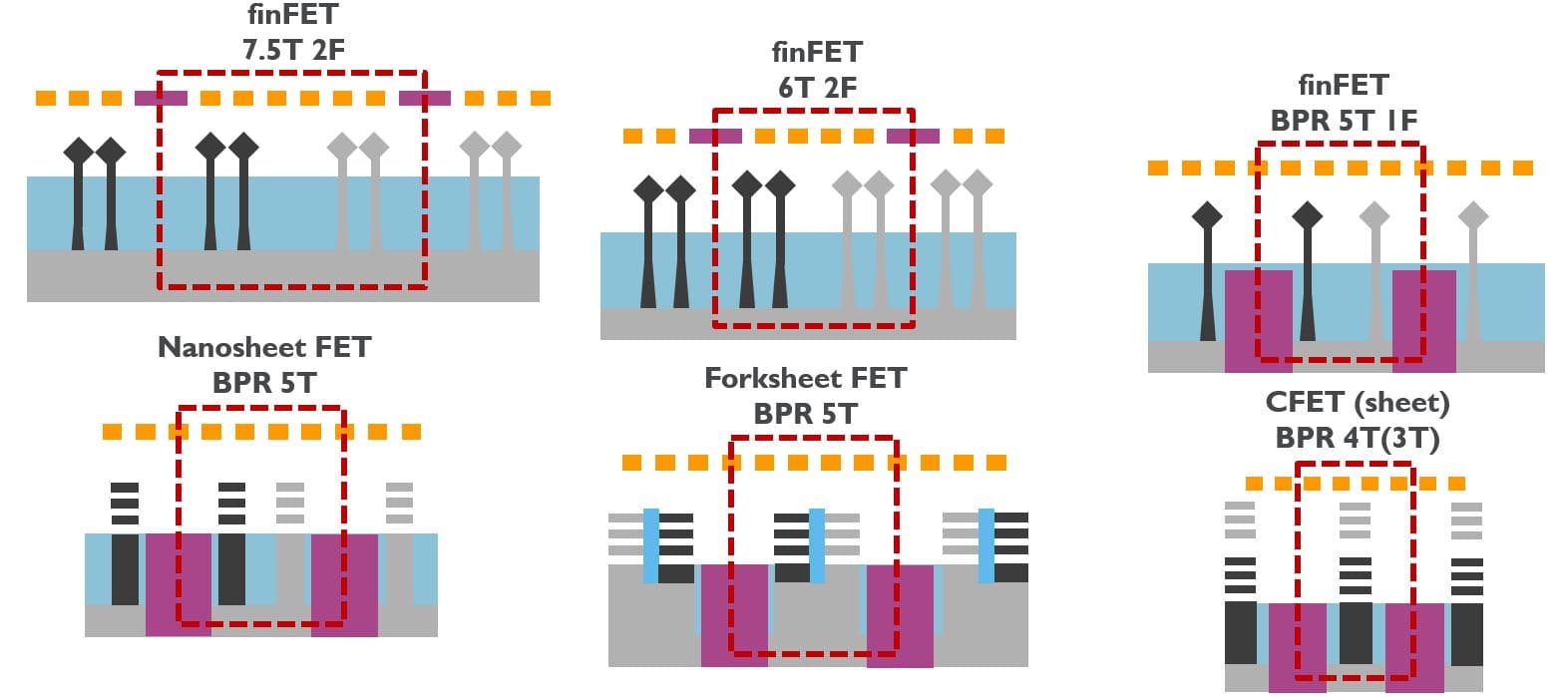
In 2012, first commercial 22nm FinFETs have been introduced. Since then, FinFET architectures were improved for enhanced performance and reduced area. For example, the 3D nature of the FinFET allowed to increase fin height to obtain a higher device drive current at the same footprint. Today, industry is ramping up production of 10nm/7nm chips with FinFETs ‘inside’. At the cell level of the most advanced nodes, standard cells with a track height of 6T (which is a measure of the cell area) feature down to 2 fins per device.
To provide academia and industry early access to the most advanced technology nodes, imec launched its open PDK, embedded in EDA tool suites. Find out more.
Vertically stacked nanosheets: an evolutionary step
But as scaling is pushed beyond 5nm, the FinFET is expected to run out of steam. At reduced gate length, the FinFET structure in turn fails to provide enough electrostatic control. On top of that, the evolution to lower track height standard cells requires a transition to single-fin devices, which cannot provide enough drive current – even if fin height is further increased.
With changing technology nodes, the semiconductor industry is however not eager to switch to other transistor architectures. Some companies might even decide to stay at certain nodes longer. But still, there are applications – such as machine learning, big data analysis and data center servers – that will require the latest ‘universal’ CMOS solutions. With such a universal CMOS solution, one and the same transistor architecture in one and the same technology node can be used to perform all functionalities on the chip.
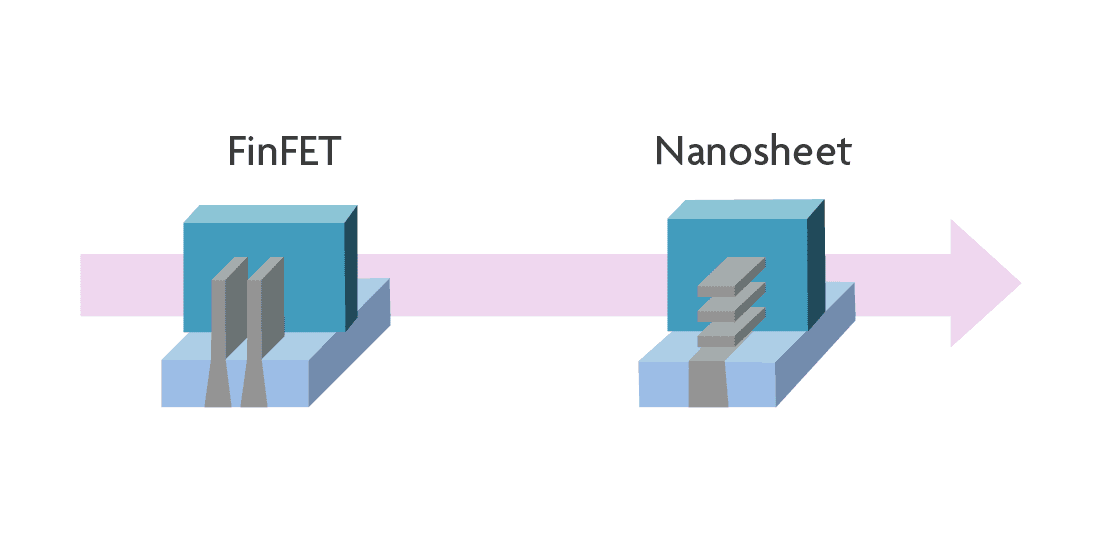
Here, vertically stacked nanosheet transistors can come to the rescue. They can be considered a natural evolution of the FinFET device. Just imagine placing a FinFET on its side, and dividing it into separate horizontal sheets, which make up the channels. A gate now fully wraps around the channel. This gate-all-around nature of the nanosheet provides superior channel control compared to the multi-gate FinFET. At the same time, the more optimal distribution of the channel cross-section in the 3D volume optimizes the effective drive per footprint.
The need for scaling boosters
The migration to nanosheet devices becomes optimal at low cell track heights of 6T and 5T, where fin depopulation would degrade drive current in traditional FinFET-based cells.
But reducing track heights (and hence, cell area) from 6T to 5T cannot happen without introducing structural scaling boosters such as buried power rails and wrap-around contacts.
Power rails provide power to the different components of the chip and are traditionally implemented as metal lines in the chip’s BEOL (i.e., the Mint and M1 layers). There, however, they occupy considerable space. In a buried power rail construct, the power rails are buried in the chip’s front-end-of-line to help free up routing resources for the interconnects. Moreover, they provide a lower resistive local distribution of the current to a technology that suffers from increasing BEOL resistance with pitch scaling. By removing the power rails from the back-end-of-line, the standard cell height can be further reduced from 6T to 5T.
The next step: reducing the spacing between p and n
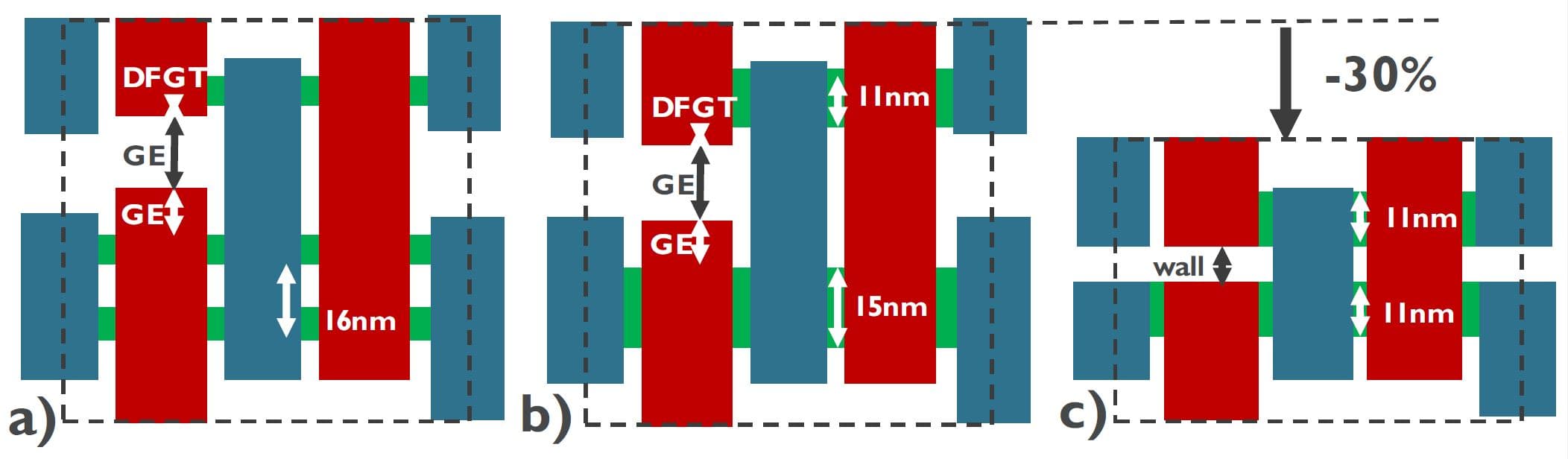
As the journey to smaller track heights continues, a further reduction of cell height will require a much tighter spacing between nFET and pFET devices within the cell. However, for both FinFET and nanosheet devices, process limitations pose a limit to how close these n and p devices can be brought together. In FinFET architectures, for example, 2 dummy fin spacings are typically required between n and p, consuming up to 40-50% of the total available space.
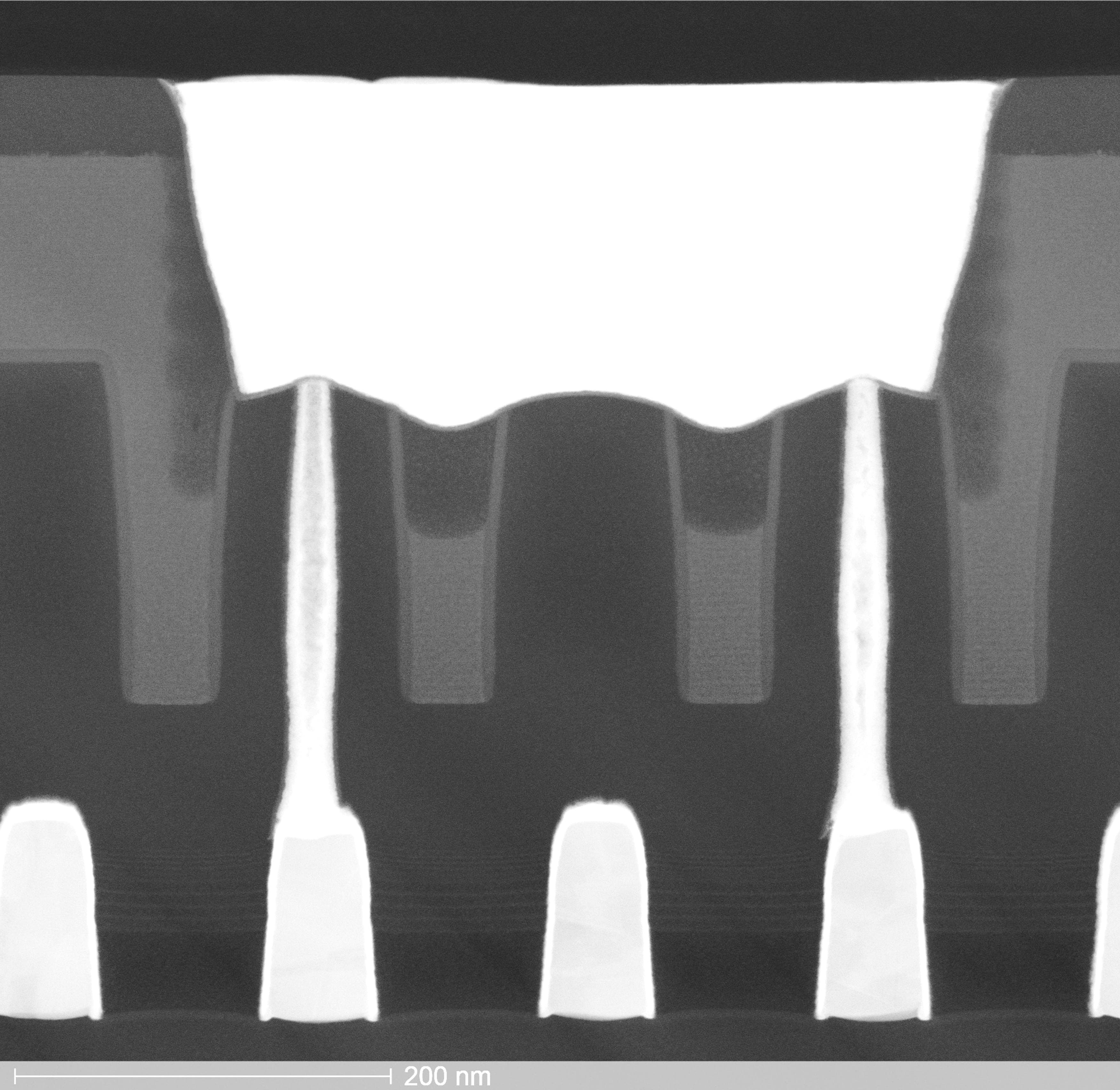
To extent the scalability of these devices, imec has recently proposed an innovative alternative architecture, called the forksheet device. The forksheet can be considered a natural extension of the nanosheet device.
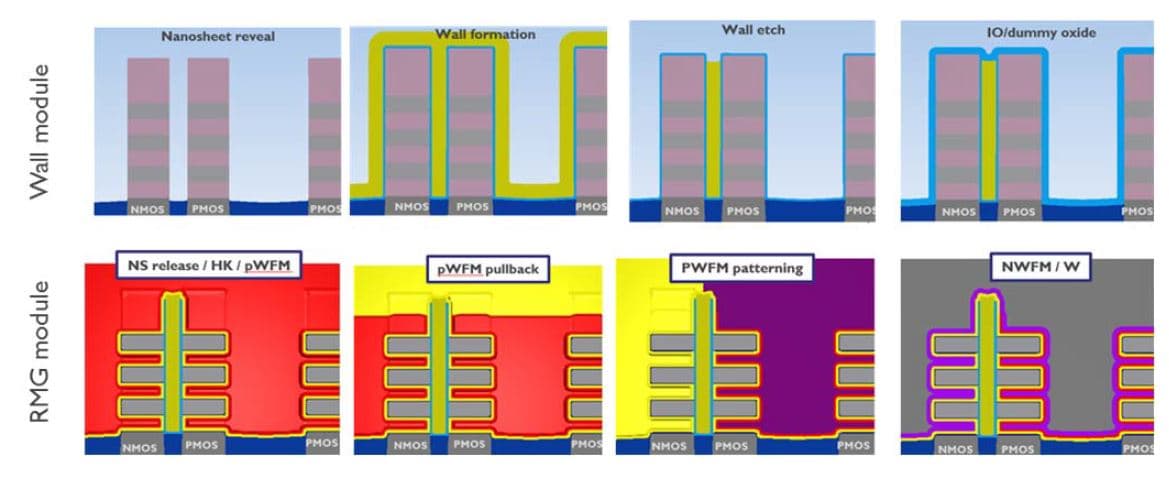
Contrary to the nanosheet device, the sheets are now controlled by a forked gate structure, realized by introducing a dielectric wall in between the p- and nMOS devices before gate patterning. This wall physically isolates the p-gate trench from the n-gate trench, allowing a much tighter n-to-p spacing.
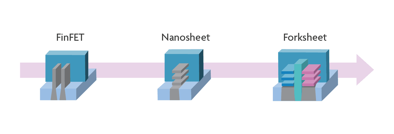
The process flow used for making the forksheet devices is similar as the one for making nanosheet devices, with only a few additional process steps. The dielectric isolation between n and p even holds a few process advantages, including, for example, a more simplified process for filling the work function metal. On top of this process window enhancement, the forksheet is expected to have superior area and performance scalability – due to the large reduction in n-to-p separation.
Forksheet device: improved performance and area
Researchers at imec have recently used TCAD simulations to quantify the expected power-performance-area (PPA) potential of the forksheet device architecture. The device under study targets imec’s 2nm technology node, using a contacted gate pitch of 42nm and a 5T standard cell library with a metal pitch of 16nm. The proposed design includes scaling boosters such as buried power rails and wrap around contacts.
Compared to a nanosheet device, a 10% speed gain (at constant power) and a 24% power reduction (at constant speed) has been calculated. This performance boost can be partly explained by a reduced (parasitic) Miller capacitance, resulting from a smaller gate-drain overlap. The available space can also be used to increase the sheet width, and as such enhance the drive current. Finally, the n-to-p separation reduction can be exploited for shrinking the track height from 5T to 4.3T – resulting in a 20% cell area reduction. When implemented in an SRAM design, the simulations reveal a combined cell area scaling and performance increase of 30%, for 8nm p-n spacing.
The forksheet can be considered a next step in the natural evolution from planar to FinFET and to vertically stacked nanosheets. The above characteristics demonstrate its potential as an ultimate logic ‘universal’ CMOS device for the 2nm technology node. In further research, the process challenges to fully bring these devices into manufacturing need to be resolved.
CFET: the road towards 3T logic standard cells
Beyond 5T, a further reduction of the cell height is now mainly limited by routability issues – which should be evaluated at the logic block level. Optimizing routability brings us to the CFET or complementary FET device – pushing the horizon for Moore’s Law further out.
The concept of CFET consists in ‘folding’ the nFET on top of the pFET (either fin-on-fin or sheet-on-sheet) – as such fully exploiting the possibilities of device scaling in 3D.
By its stacked nature, the CFET exhibits 2 levels of local interconnects – providing more freedom for internal cell routing and for reducing cell area. Routing between cells can also be largely improved.
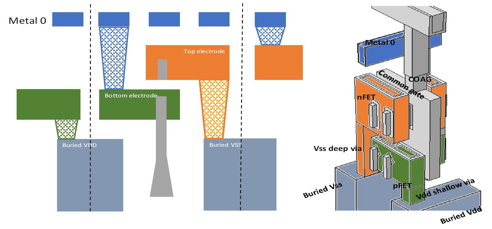
First assessments have shown that a FinFET-based 4T CFET can match and even surpass the standard cell power-performance metrics of a 5T ‘standard’ FinFET device. It can also yield standard cells and SRAM cells with 25% smaller layout area. A nanosheet-based CFET could offer an extra performance boost and be necessary for scaling down to a 3T logic standard cell.
Conclusion
In this article, imec has mapped out an evolutionary path towards ultimately scaled logic devices for 2nm and beyond technology nodes. After today’s mainstream FinFET comes the nanosheet device, offering superior channel control with limited additional process complexity. When complemented with scaling boosters, standard cells with 5T track height come within reach. As a next step, the forksheet may enter the scene, offering a path to 4.3T cells due to a reduced n-to-p spacing. First simulations confirm its potential for the 2nm technology node. The CFET completes the roadmap as the ultimate compact CMOS structure, holding promise for 3T logic standard cells.
Want to know more?
- Read imec’s press release on the forksheet device.
- At IEDM 2019, imec presented two papers related to the postFinFET era: (1) ‘Enabling sub-5nm CMOS technology scaling – thinner and taller!’ (invited paper) by J. Ryckaert et al., and (2) ‘Novel forksheet architecture as ultimate logic scaling device towards 2nm’, by P. Weckx et al. You can request these articles via our contact form.
Authors

Julien Ryckaert
Julien Ryckaert received the M.Sc. degree in electrical engineering from the University of Brussels (ULB), Belgium, in 2000 and the PhD degree from the Vrije Universiteit Brussel (VUB) in 2007. He joined imec as a mixed-signal designer in 2000 specializing in RF transceivers, ultra-low power circuit techniques and analog-to-digital converters. In 2010 he joined the process technology division in charge of design enablement for 3DIC technology. Since 2013, he is in charge of imec’s design-technology co-optimization (DTCO) platform for advanced CMOS technology nodes. He is now program director focusing on scaling beyond the 3nm technology node as well as the 3D scaling extensions of CMOS.
Discover more


Sony and imec unveil high-density backside connectivity module enabling next-generation 3D chip integration
Read more

ASML, TSMC and imec bring industry-ready 2D-material transistors closer with breakthrough 300mm integration
Read more