Julien Ryckaert
Julien Ryckaert received the M.Sc. degree in electrical engineering from the University of Brussels (ULB), Belgium, in 2000 and the PhD degree from the Vrije Universiteit Brussel (VUB) in 2007. He joined imec as a mixed-signal designer in 2000 specializing in RF transceivers, ultra-low power circuit techniques and analog-to-digital converters. In 2010 he joined the process technology division in charge of design enablement for 3DIC technology. Since 2013, he is in charge of imec’s design-technology co-optimization (DTCO) platform for advanced CMOS technology nodes. He is now program director focusing on scaling beyond the 3nm technology node as well as the 3D scaling extensions of CMOS.

Authored articles
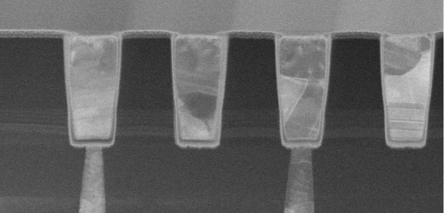
A path to high-density front- and backside wafer connectivity
Advances in wafer-to-wafer hybrid bonding and backside technologies take CMOS 2.0 from concept to reality, offering more options for compute system scaling
Read more
CMOS 2.0: bringing heterogeneity inside the system-on-chip
A new approach to miniaturization with greater versatility for compute system optimization
Read more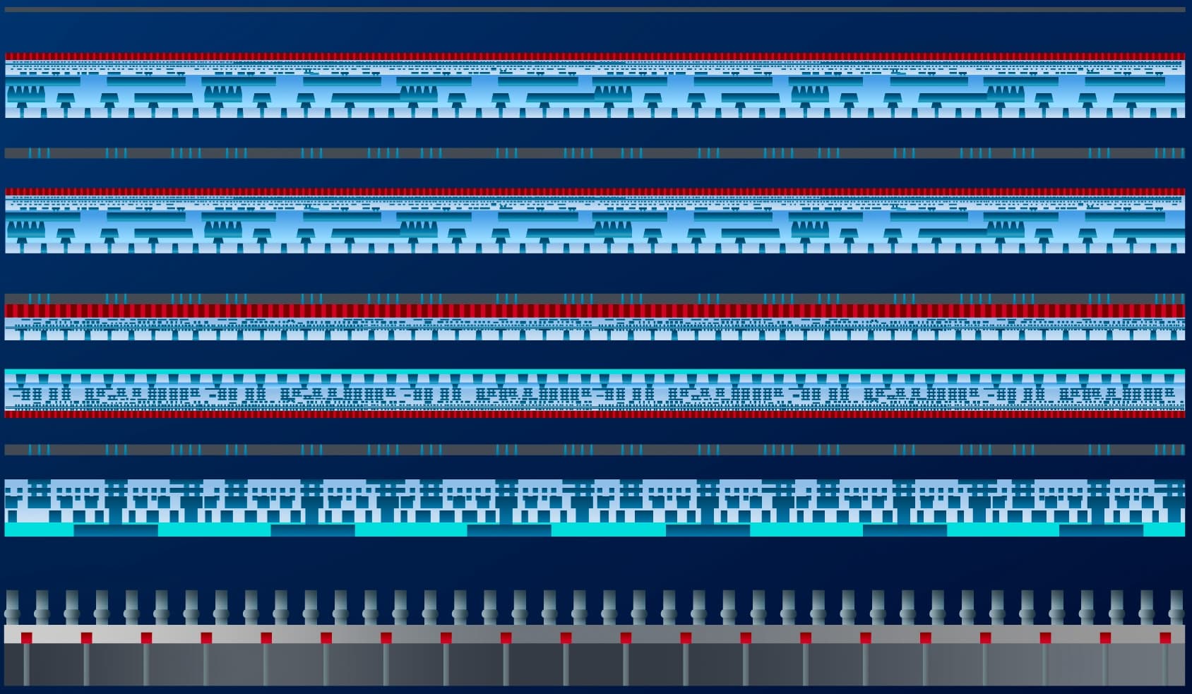
The CMOS 2.0 Revolution
CMOS faces unprecedented scaling and cost challenges. This requires us to reimagine the existing paradigm.
Read more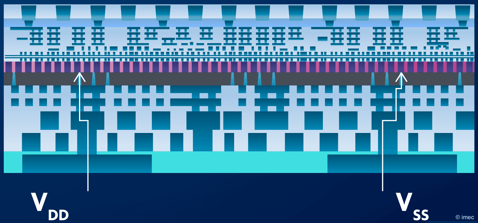
Backside power delivery options: a DTCO study
Imec highlights the potential of backside power delivery for high-performance computing and evaluates options for backside connectivity
Read more
System-technology co-optimization (STCO): unlocking system-scaling bottlenecks
System-technology co-optimization (STCO): translating future system needs into technology requirements in a top-down approach
Read moreImec puts complementary FET (CFET) on the logic technology roadmap
Improved process flows make sequential CFET an attractive alternative to monolithic CFET.
Read more