Novel SOT-MRAM architecture opens doors to high-density last-level cache memory applications
First demonstration of field-free, gate-voltage assisted SOT-based switching operation in a multi-pillar configuration

In short
Today, three main issues challenge the use of spin-orbit torque magneto-resistive random-access memory (SOT-MRAM) devices in last-level cache memory applications: scalability, dynamic power consumption, and the need for a manufacturable compact field-free switching solution.
At the 2022 IEDM, imec presented a novel SOT-MRAM architecture that solves these issues in one go.
The design improvements, in combination with a high switching speed and >1012 endurance, make the novel device an attractive alternative to SRAM in embedded memory applications.
SOT-MRAM: sub-ns switching speed, high endurance
In recent years, the chip industry has become increasingly interested in SOT-MRAM technology development. SOT-MRAM is a non-volatile memory with promising properties for embedded memory applications, such as L3 (and above) cache memory in high-performance computing and mobile applications. Today, this role is usually fulfilled by ultrafast volatile static RAM (SRAM) but scaling constraints limiting SRAM bit density force the memory community to look for alternatives. In addition, SRAM bit cells increasingly suffer from power dissipation when the memory is inactive, compromising a low standby power. Non-volatile memories such as MRAM not only have the potential to offer smaller bit cells. Their non-volatile nature would also solve the standby power issue.
SOT-MRAM has evolved out of the more mature spin-transfer torque MRAM (STT-MRAM), with better prospects for cache applications due to a larger endurance and faster switching between two binary states. In both MRAM flavors, a magnetic tunnel junction (MTJ) makes up the ‘heart’ of the memory cell. In this MTJ, a thin dielectric layer (MgO) is sandwiched between a ferromagnetic fixed layer (CoFeB) and a ferromagnetic free layer (CoFeB). Writing of the memory cell is performed by switching the magnetization of the free layer – the ‘storage’ layer of the MRAM bit cell. For reading, the magnetoresistance of the MTJ is measured by passing a current through the junction. This tunnel magnetoresistance (TMR) can be high or low, depending on the relative orientation of the magnetizations of the free and fixed layers (i.e., parallel (1) or antiparallel (0)).
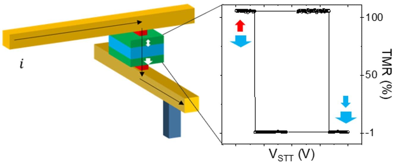
The main difference between STT- and SOT-MRAM resides in the current injection geometry used for the write process. While in STT-MRAM, the current is injected perpendicularly into the MTJ, current injection in SOT-MRAM happens in-plane, in an adjacent SOT layer – typically a heavy metal such as tungsten (W). Hence, in SOT-MRAM, the read and write paths are de-coupled, significantly improving the device’s endurance and read stability. The in-plane current injection also removes the switching delay characteristic of STT-MRAM operation. In 2018, imec was the first to demonstrate reliable SOT-MRAM switching down to 210ps, with excellent endurance (>5x10¹⁰ switching cycles) and 300pJ operation power.
SOT-MRAM challenges: area consumption, high injection current, manufacturability
Being non-volatile, SOT-MRAM offers a significantly lower standby power than SRAM at high cell density. But the dynamicpower is still relatively high due to the large current needed for the write operation.
In addition, innovations in density scaling are needed to make SOT-MRAM a true competitor for SRAM in embedded memory applications. Adopting a perpendicular magnetization in the fixed and free layers (referred to as p-MTJ) instead of a traditional in-plane magnetization improves the scaling potential, as it removes the need for the memory cell to be rectangular.
But the key challenge lies in the device architecture. STT-MRAM with its pillar-like structure is a two-terminal device. When implemented in a memory array configuration, only one select device – usually an (access) transistor – per MTJ cell is needed to select the memory element for either reading or writing. SOT-MRAM with its separate read and write paths is a three-terminal device. In this case, two access transistors are needed for each memory element, one to select for the read operation, one for the write operation. So, while independent read and write paths provide an additional benefit for reliability, they consume additional space due to the extra access transistor which comes with additional metal wires.
And there is also the manufacturability. In 2018, imec demonstrated full-scale integration of SOT-MRAM device modules on 300mm wafers using CMOS-compatible processes – facilitating industrial uptake. But the practical implementation of a SOT-MRAM p-MTJ bit cell remains hampered by the need for an extra in-plane magnetic field during the write operation. This magnetic field is required to break the symmetry and ensure deterministic magnetization switching. In other words, without this magnetic field, it’s impossible to know what state the free layer ends up in after applying the write current. During the SOT-MRAM development phase, this field can be generated by an external magnetic field, but the final devices will require a robust and compact field generation at the device location.
Key improvement steps
So far, solutions for each of the individual challenges have been successfully demonstrated – several pioneered by imec and demonstrated on 300mm wafers.
The role of the external magnetic field can be resumed by embedding a ferromagnet in the hard mask used to shape the SOT layer – as such eliminating the need for an external magnetic field. The ferromagnet induces a small homogeneous in-plane field on the free layer of the magnetic tunnel junction. In 2019, imec showed that this ‘field-free’ switching approach is reliable while preserving the sub-ns writing of the SOT-MRAM device.
Problems associated with the high write current can be partly relieved by adopting a voltage-gate (VG) assisted approach. In such a VG-SOT-MRAM device, the SOT effect is again responsible for switching the free layer – using an in-plane current for the actual switching. But a voltage-controlled magnetic anisotropy (VCMA) gate now assists its operation by evoking an electric field (across the tunnel barrier) to lower the energy barrier. As such, a smaller current is needed for the write operation, improving dynamic power consumption.
An added beauty of the VG-assisted approach is that it opens doors towards multi-pillar/multi-bit device structures. Instead of connecting one MTJ pillar to an SOT track, four (or more) MTJ pillars can now be implemented on top of a shared SOT track. Within this multi-pillar, multi-bit device, an individual pillar (or bit) can be selected by applying a voltage on its VCMA gate. This induces a reduction of its energy barrier, facilitating switching. But only one single (big) access transistor (instead of four) is needed to write through the shared SOT track. And this leads to an overall more compact bit cell.
But so far, field-free solutions that are fully compatible with a multi-pillar operation have not been demonstrated. For example, as presented above, the solution for field-free switching requires embedding a ferromagnet in each of the p-MTJ pillars, largely compromising scalability.
Putting the pieces together: field-free, gate-voltage assisted SOT-MRAM in a multi-pillar configuration
At IEDM 2022, imec demonstrated a novel, fully functional multi-pillar SOT-MRAM device that addresses all the above challenges in one go.
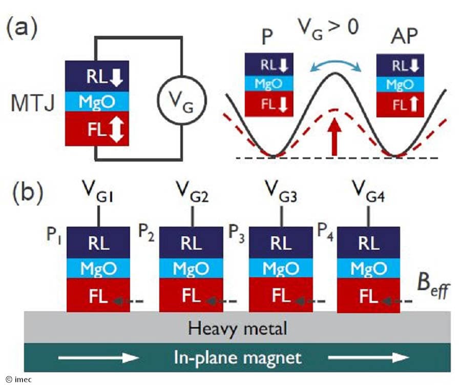
First, the device implements a scalable, field-free solution by implementing an in-plane magnetic layer within the common SOT track – referred to as a hybrid spin source. This extra common in-plane magnetic layer couples to each individual memory element. It acts like a magnetic field for each pillar but is no longer part of each individual MTJ stack, improving scalability.
Second, the VCMA effect assists in the write operation by modulating and lowering the energy barrier for the actual switching, resulting in a lower switching energy.
And third, this VCMA-assisted concept reduces the number of transistors required per bit, benefitting area consumption and scalability.
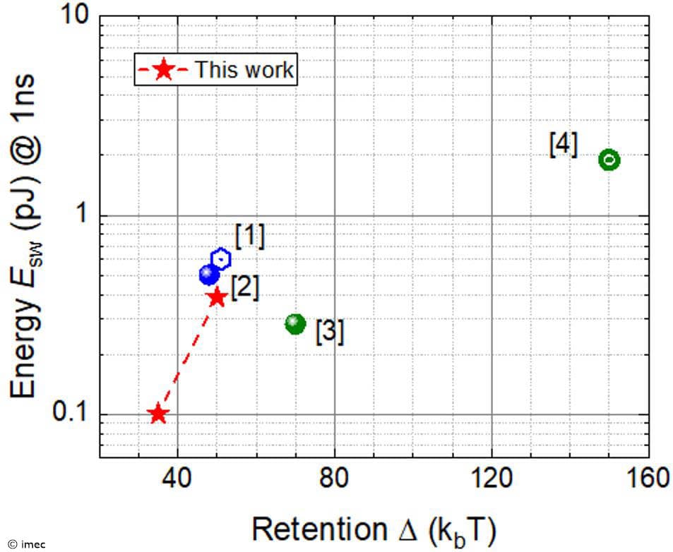
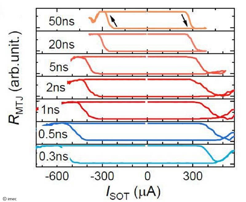
This device approach enables field-free switching with high switching efficiency (60fJ/bit power consumption), fast operational speed (down to 300ps), and >1012endurance. It is suitable for both one-pillar and multi-bit SOT devices, and the 300mm integrated technology is CMOS and back-end-of-line compatible.
Towards industrial adoption
The above characteristics make the novel, non-volatile SOT-MRAM device an attractive alternative for high-density last-level embedded cache applications.
A few additional developments are needed before this non-volatile SOT-MRAM memory can be brought to the market. Current work focuses on further lowering the switching energy by improving both the SOT track and MTJ pillar stack designs. In addition, the imec team is working toward array configurations of SOT-MRAM devices and progressing that technology towards industrialization.
One can also envision the SOT-MRAM memory becoming part of a separate off-chip cache die, bonded together to the logic and/or lower-level cache memories using die-to-die or die-to-wafer bonding techniques – conceptually similar to AMD’s 3D V-CacheTM technology with 3D stacked SRAM cache die. This off-chip solution is independently optimized on a separate die and promises to be more cost-efficient than traditional last-level embedded cache implementations.
This article was originally published in EETimes Europe.
Authors

Sebastien Couet
Sebastien Couet received his PhD in physics from the University of Hamburg, Germany, in 2008. From 2009 to 2014, he was a postdoctoral fellow at the Katholieke Universiteit Leuven, Belgium, where he specialized in the interface physics of magnetic/oxide heterostructures. In 2014, he joined imec, Leuven, where he is currently the program director for magnetics. In this role, he oversees the development of the various MRAM-based memory concepts for embedded and standalone applications and other exploratory magnetic device concepts.

Gouri Sankar Kar
Gouri Sankar Kar received the PhD degree in semiconductor device physics from the Indian Institute of Technology, Khragput, India in 2002. From 2002 to 2005, he was a visiting scientist at Max Planck Institute for Solid State Research, Stuttgart, Germany, where he worked with Nobel Laureate (1985, Quantum Hall Effect) Prof. Klaus von Klitzing on quantum dot FET. In 2006, he joined Infineon/Qimonda in Dresden, Germany as lead integration engineer. There he worked on the vertical transistor for DRAM application. In 2009, he joined imec, Leuven, Belgium, where he is currently distinguished member of technical staff (DMTS). In this role, he defines the strategy and vision for RRAM, DRAM-MIMCAP and STT-MRAM programs both for stand-alone and embedded applications.
Discover more

Imec achieves breakthroughs in ferroelectric memory research for next-generation memory solutions to meet AI-era data needs
Read more
Imec demonstrates the first 3D implementation of a charge coupled device for AI memory applications
Read more