Gouri Sankar Kar
Gouri Sankar Kar received the PhD degree in semiconductor device physics from the Indian Institute of Technology, Khragput, India in 2002. From 2002 to 2005, he was a visiting scientist at Max Planck Institute for Solid State Research, Stuttgart, Germany, where he worked with Nobel Laureate (1985, Quantum Hall Effect) Prof. Klaus von Klitzing on quantum dot FET. In 2006, he joined Infineon/Qimonda in Dresden, Germany as lead integration engineer. There he worked on the vertical transistor for DRAM application. In 2009, he joined imec, Leuven, Belgium, where he is currently distinguished member of technical staff (DMTS). In this role, he defines the strategy and vision for RRAM, DRAM-MIMCAP and STT-MRAM programs both for stand-alone and embedded applications.
Authored articles
Disrupting the DRAM roadmap with capacitor-less IGZO-DRAM technology
2T0C IGZO-based DRAM opens doors to high-density 3D DRAM and embedded DRAM
Read more
Introducing 2D-material based devices in the logic scaling roadmap
A path from planar 2D-FETs to high-performance 2D-CFETs
Read more
Bringing SOT-MRAM technology closer to last-level cache memory specifications
Device performance improvement, full array integration, and increased understanding of magnetic immunity
Read moreThe promise of OTS-only memories for next-gen compute system architectures
The discovery of a memory effect in ovonic threshold switching (OTS) devices paves the way to a new compute express link (CXL) memory
Read more
The promise of OTS-only memories for next-gen compute system architectures
The discovery of a memory effect in ovonic threshold switching (OTS) devices paves the way to a new compute express link (CXL) memory
Read moreIGZO-based DRAM for energy- and area-efficient analog in-memory computing
First experimental demonstration of multilevel, multiply accumulate operations on IGZO-based 2-transistor-1-capacitor (2T1C) and 2T0C cells
Read moreNovel SOT-MRAM architecture opens doors to high-density last-level cache memory applications
First demonstration of field-free, gate-voltage assisted SOT-based switching operation in a multi-pillar configuration
Read more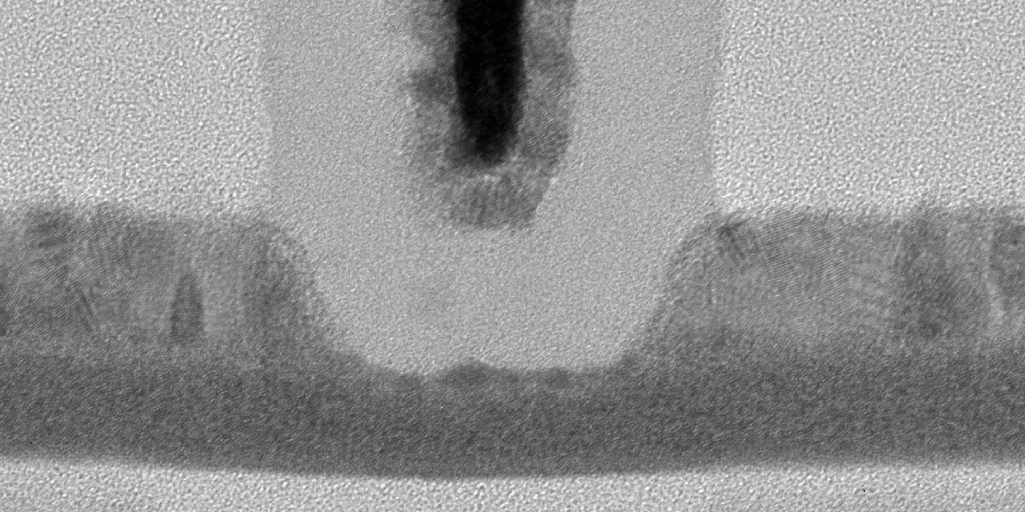
Capacitor-less IGZO-based DRAM cell with excellent retention, endurance and gate length scaling
Device architecture improvement is complemented with new insights in IGZO transistor reliability
Read more
MRAM technologies: from space applications to unified cache memory?
Towards CMOS-compatible fabrication of STT-, SOT-, VCMA-, VG-SOT- and domain-wall flavors of MRAM
Read more