Capacitor-less IGZO-based DRAM cell with excellent retention, endurance and gate length scaling
Device architecture improvement is complemented with new insights in IGZO transistor reliability
In short
Capacitor-less indium-gallium-zinc-oxide (IGZO)-based DRAM cell architectures show great potential for realizing high-density 3D DRAM memories.
In this article, Gouri Sankar Kar, memory program director at imec, reveals an IGZO-based DRAM cell that has excellent specifications for DRAM memory applications – thanks to an optimization of the IGZO transistor architecture. In addition, he shows the first lifetime estimation of the DRAM cell’s key components, based on new insights into the reliability of IGZO thin-film transistors.
The results are presented in two papers at the 2021 IEEE International Electron Devices Meeting (IEDM).
Towards high-density 3D DRAM
At last year’s International Electron Devices Meeting (2020 IEDM), imec demonstrated for the first time a capacitor-less dynamic random access memory (DRAM) cell, implementing two indium-gallium-zinc-oxide (IGZO) thin-film transistors (TFTs) and no capacitor. This novel 2-transistor-0-capacitor (2T0C) DRAM cell architecture promises to overcome the key obstacles for classical 1-transistor-1-capacitor (1T1C) DRAM density scaling, i.e., the large off-current of Si transistors at small cell sizes, and the large area consumed by the storage capacitor. In a 2T0C IGZO-TFT DRAM cell, there is no need for a storage capacitor, as the parasitic capacitance of the read transistor serves as the storage element. In addition, IGZO-TFTs are known for their very low off-current, leading to enhanced retention of the memory cell. Finally, the ability to process IGZO-TFTs in the back-end-of-line (BEOL) allows to reduce the DRAM memory’s footprint (by moving the memory cell under the memory array) and to stack individual DRAM cells – hence providing a path towards high-density 3D DRAM. This evolution is needed to continue to provide sufficient DRAM capacity for data-intensive applications (such as artificial intelligence, internet-of-things, data centers and cloud computing).
In 2020, a first 2T0C IGZO-based DRAM cell with >400s retention time could be demonstrated, which led to significantly reduced refresh rate and power consumption compared to classical DRAM variants. The devices were manufactured on 300mm wafers, and gate lengths were scaled down to 45nm. However, in this first ‘conceptual’ demonstration, the IGZO TFTs were not optimized for maximal retention, and an assessment of the endurance (i.e., the number of read/write cycles before failure) was still missing. Also, at that time, no accurate model existed for predicting the lifetime of the IGZO devices.
>103s retention, unlimited endurance and gate length scalability down to 14nm
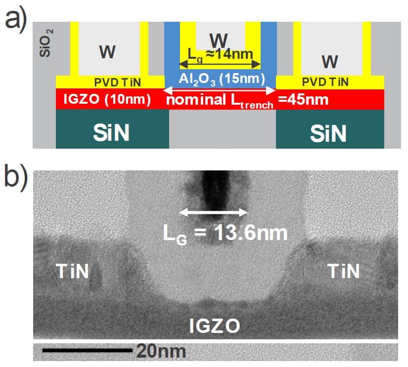
At the 2021 IEDM, imec presents a fully 300mm BEOL compatible IGZO-based capacitorless DRAM cell with improved specifications, i.e., >103s retention and unlimited (>1011) endurance. These results were obtained after selecting the most optimal integration scheme for the single IGZO transistors, i.e., a gate-last integration scheme with buried oxygen tunnel and self-aligned contacts. The implementation of a buried oxygen tunnel in combination with an anneal in O2 ambient was proven to reduce the oxygen-vacancy concentration in the IGZO channel without impacting the series resistance at source and drain region – leading to larger on-current and lower off-current.
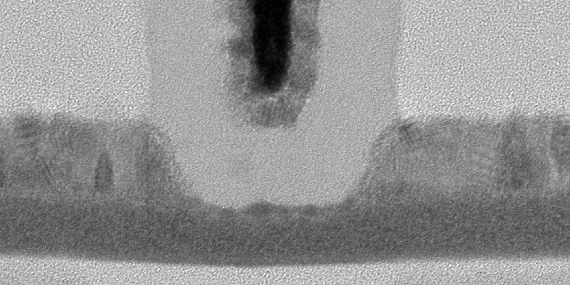
With this architecture, the gate length of the IGZO TFT could be scaled down to an unprecedented 14nm, while still preserving >100s retention. The retention at small gate length could be further optimized by controlling the threshold voltage (Vt) through equivalent oxide thickness (EOT) scaling, by contact resistance improvement and by reducing the IGZO layer thickness. When the latter thickness is reduced to 5nm, the oxygen tunnel and anneal step in O2 can even be omitted – leading to a much-simplified integration approach.
More details on the selected integration approach and on the achieved device specifications are described in the 2021 IEDM paper ‘Tailoring IGZO-TFT architecture for capacitorless DRAM, demonstrating >103s retention, >1011 cycles endurance and Lg scalability down to 14nm’ by A. Belmonte et al.
Lifetime estimation based on PBTI reliability modelling
So far, an accurate model for predicting the IGZO-based DRAM lifetime is lacking since the IGZO TFT’s degradation mechanisms are not fully understood. IGZO transistors are inherently n-type devices, and this points to positive bias temperature instability (PBTI) as possibly the main degradation mechanism.
PBTI is a well-known aging mechanism in Si n-type metal-oxide-semiconductor field-effect transistors (MOSFETs) where it can severely affect the device performance and reliability. It typically manifests itself as an undesirable shift of the device threshold voltage and a decrease of the drain current. For these Si-based devices, PBTI is ascribed to the presence of electron traps in the gate dielectric, trapping charge carriers from the device conduction channel.
Most of the existing reliability assessments on IGZO TFTs neglect however the impact of the gate dielectric. Imec has for the first time studied the impact of the gate dielectric on the PBTI of IGZO TFTs. The results are summarized in the 2021 IEDM paper ‘Understanding and modelling the PBTI reliability of thin-film IGZO transistors’, by A. Chasin et al.
The team found that four different mechanisms play a role in the degradation process, each with different time kinetics and activation energies. They can be mainly ascribed to both electron trapping in the gate dielectric, and to the release of hydrogen species from the gate dielectric into the IGZO channel during PBTI stress.
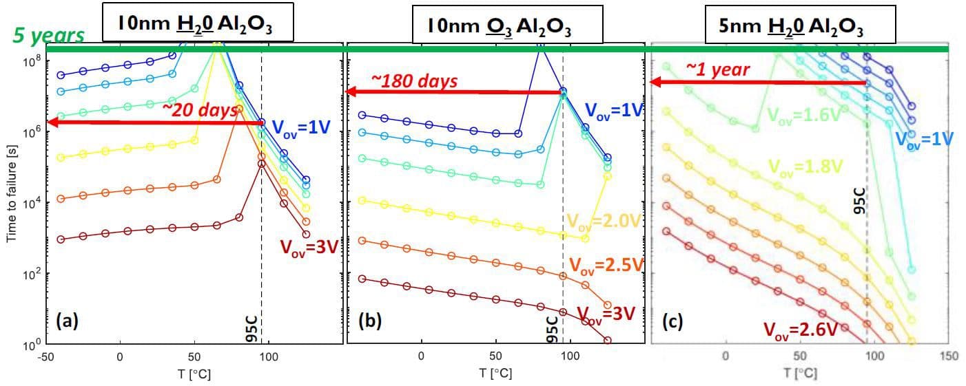
The imec team has combined these multiple degradation mechanisms into a model, which makes it possible to predict the IGZO TFT lifetime at target operation conditions. The model is found to fit to experimental data and can be used to propose optimizations for enhancing the lifetime. For example, by reducing the gate dielectric thickness, the predicted time to failure can be enhanced from about 20 days to about one year.
Conclusion
Improvements to the IGZO-based DRAM cell architecture and integration have enabled 2T0C DRAM memory cells with >103 retention, unlimited endurance and gate length scaling down to 14nm. These specifications make capacitor-less IGZO-DRAM a suitable candidate for realizing high-density 3D DRAM memories. The device improvements were complemented with new insights into the IGZO TFT’s reliability, revealing different degradation mechanisms responsible for the PBTI. These formed the key ingredients of an accurate model with which the lifetime of the DRAM memory’s key components can be predicted.
Want to know more?
- Appeared in EE Times Europe
- Follow imec's presence at the 2021 IEEE International Electron Devices Meeting
- ‘Imec demonstrates capacitor-less IGZO-based DRAM cell with >400s retention time’, press release 2020 IEDM;
- ‘First demonstration of sub-12nm Lg gate last IGZO-TFTs with oxygen tunnel architecture for front gate devices’, by S. Subhechha et al, 2021 VLSI paper.
- ‘Tailoring IGZO-TFT architecture for capacitorless DRAM, demonstrating >103s retention, >1011 cycles endurance and Lg scalability down to 14nm’, by A. Belmonte et al., 2021 IEDM paper;
- ‘Understanding and modelling the PBTI reliability of thin-film IGZO transistors’, by A. Chasin et al., 2021 IEDM paper.
Interested in receiving the 2021 IEDM papers on IGZO-DRAM? Fill in our contact form.
Authors

Gouri Sankar Kar
Gouri Sankar Kar received the PhD degree in semiconductor device physics from the Indian Institute of Technology, Khragput, India in 2002. From 2002 to 2005, he was a visiting scientist at Max Planck Institute for Solid State Research, Stuttgart, Germany, where he worked with Nobel Laureate (1985, Quantum Hall Effect) Prof. Klaus von Klitzing on quantum dot FET. In 2006, he joined Infineon/Qimonda in Dresden, Germany as lead integration engineer. There he worked on the vertical transistor for DRAM application. In 2009, he joined imec, Leuven, Belgium, where he is currently distinguished member of technical staff (DMTS). In this role, he defines the strategy and vision for RRAM, DRAM-MIMCAP and STT-MRAM programs both for stand-alone and embedded applications.
Discover more

Imec achieves breakthroughs in ferroelectric memory research for next-generation memory solutions to meet AI-era data needs
Read more

Imec demonstrates the first 3D implementation of a charge coupled device for AI memory applications
Read more