Unlocking z-pitch scaling for next-generation 3D NAND flash
Airgap integration and charge trap layer separation: critical technologies for increasing the number of word-line layers

In short
Today, 3D NAND flash products are offered with over 300 stacked oxide/word-line layers to meet the demand for bit storage capacity.
The memory industry continues to increase this impressive number of layers but cannot do so without complementary ‘scaling boosters.’
One of these scaling boosters is z-pitch scaling, which involves a reduction of the oxide/word-line layer thickness to allow more layers to be stacked at a manageable cost.
Imec is developing two key technologies that enable z-pitch scaling without compromising memory operation and reliability: airgap integration and charge trap layer separation.
NAND flash, industry’s primary storage technology
Since its introduction into the memory market in the late 1980s, NAND flash has revolutionized the way we store and retrieve large amounts of data. This popular memory technology, architecturally optimized for high-density data storage, is present in all major electronic end-use markets, including smartphones, data servers, and PCs. You will also find the technology inside most removable and portable memory devices such as SD cards and USB drives. The memory is non-volatile, allowing photos, videos, audio files, archived emails and other documents to be stored and retrieved for up to ten years. More recently, NAND flash technology also plays an important role in AI and machine learning. For example, by providing efficient storage for the huge amounts of data needed for training an AI model.
NAND flash storage technology owes its success to the ability to continuously scale memory cell density and cost. Year after year, the NAND flash industry has substantially improved bit storage density, expressed in terms of increasing Gbit/mm2. Several innovations have been implemented to maintain this trend line. The move from 2D to 3D NAND flash, the increase of the number of bits per cell (up to four in commercial NAND flash memory), and the transition from the floating gate transistor to the charge trap cell for the memory operation are among the most significant developments.
A 3D gate-all-around cell architecture: the workhorse of the NAND flash industry
3D NAND flash with memory cells in a gate-all-around (GAA) vertical architecture is the industry’s workhorse for high-density data storage applications. In this 3D architecture, the memory cells are stacked to form a vertical string, and cells are addressed by horizontal word-lines.
In most 3D NAND products, the charge trap cell acts as the storage element. This memory cell resembles a MOSFET transistor with the addition of a thin layer of silicon nitride (SiN) inserted inside the transistor’s gate oxide. This turns the gate oxide into an oxide-nitride-oxide or ONO stack, the layers serving as the blocking oxide, trapping nitride, and tunnel oxide, respectively. The SiN layer contains many charge-trapping sites that can hold an electrical charge. When the gate electrode is biased positively, electrons from the channel region tunnel through the oxide layer and get trapped in the SiN layer. This raises the threshold voltage of the transistor. The state of the cell can be measured by applying a voltage across the source/drain nodes. If current flows, this means that no electrons are trapped: the cell is in a ‘1’ state. If no current is measured, cells are in the ‘trapped-electrons’ or ‘0’ state.
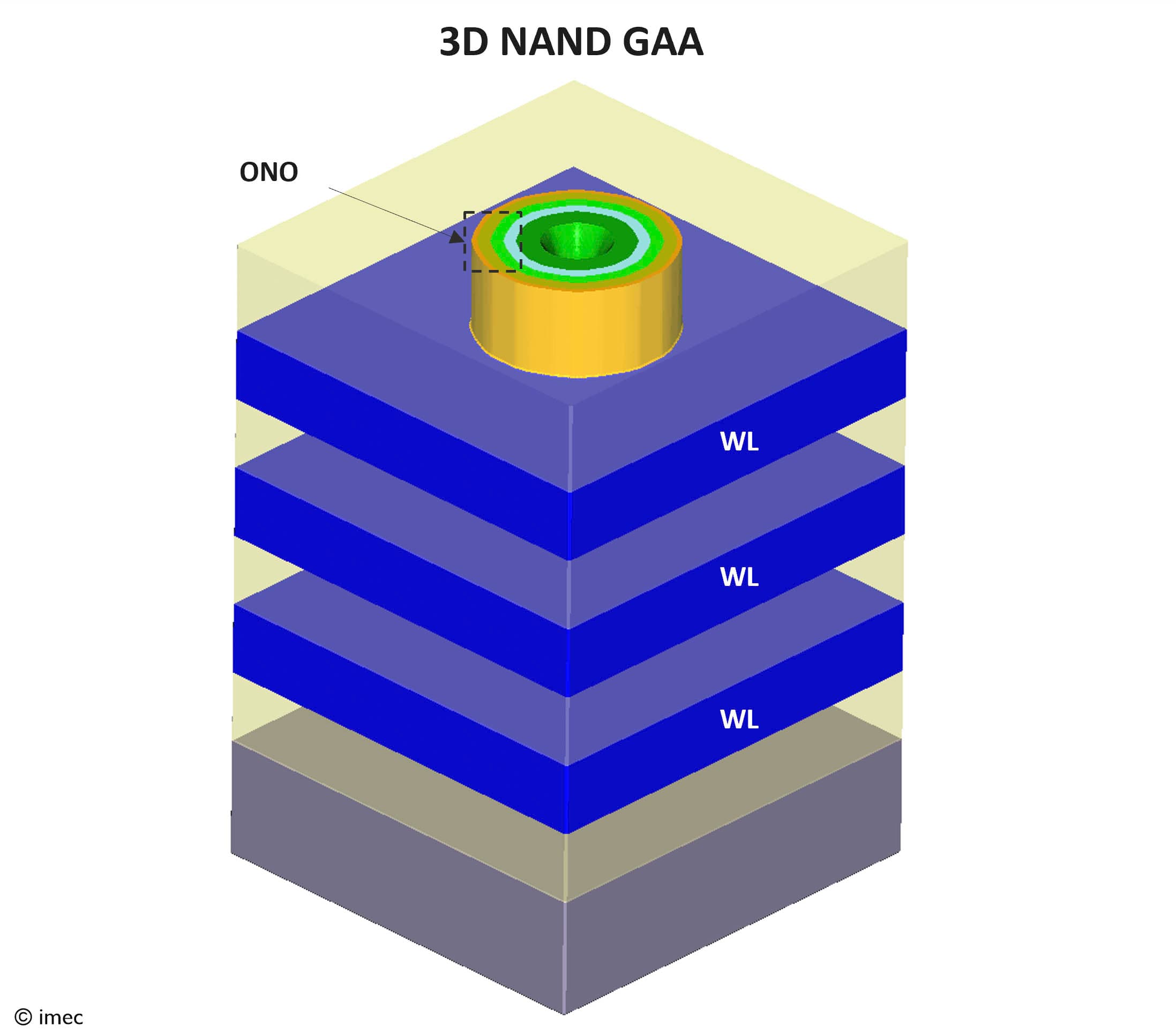
The charge trap cell is implemented in the 3D NAND structure using a GAA vertical channel method. Imagine rotating the planar transistor structure over 90 degrees, with the now vertical poly-Si conduction channel surrounded by the gate stack.
The GAA fabrication starts with growing a stack of Si-oxide/word-line layers. Next, cylindrical holes are formed by drilling down through the stack using advanced dry etch tools. The oxide and trapping layers and the poly-Si channel are then deposited along the sidewalls of the holes. This arrangement is often referred to as the macaroni channel.
Continuing the NAND flash roadmap with more oxide/word-line layers
In the years to come, the memory industry will push the GAA-based NAND flash roadmap to its ultimate limits. Today, major players offer 3D NAND flash-based products with over 300 oxide/word-line layers stacked on top of each other [1]. This number will further increase, with about 1,000 layers projected by 2030 – the equivalent of 100Gbit/mm2 [2]. But ensuring a consistent diameter string through this ~30µm-thick layer stack induces ever higher processing complexity and cost, challenging the tall stack deposition and high-aspect-ratio etch steps.
Complementary ‘scaling boosters’ are therefore added to the toolbox. These include increasing the number of bits per cell, reducing the x-y pitch of the GAA cell (lateral scaling), enhancing the area efficiency of the memory array, and module stacking. Another trend is to optimize the peripheral CMOS circuitry on a different wafer and attach it to the memory array stack using hybrid bonding techniques. To control the growing processing costs, an additional scaling is pursued in the vertical direction, referred to as z-pitch scaling.
Z-pitch scaling: benefits and pitfalls
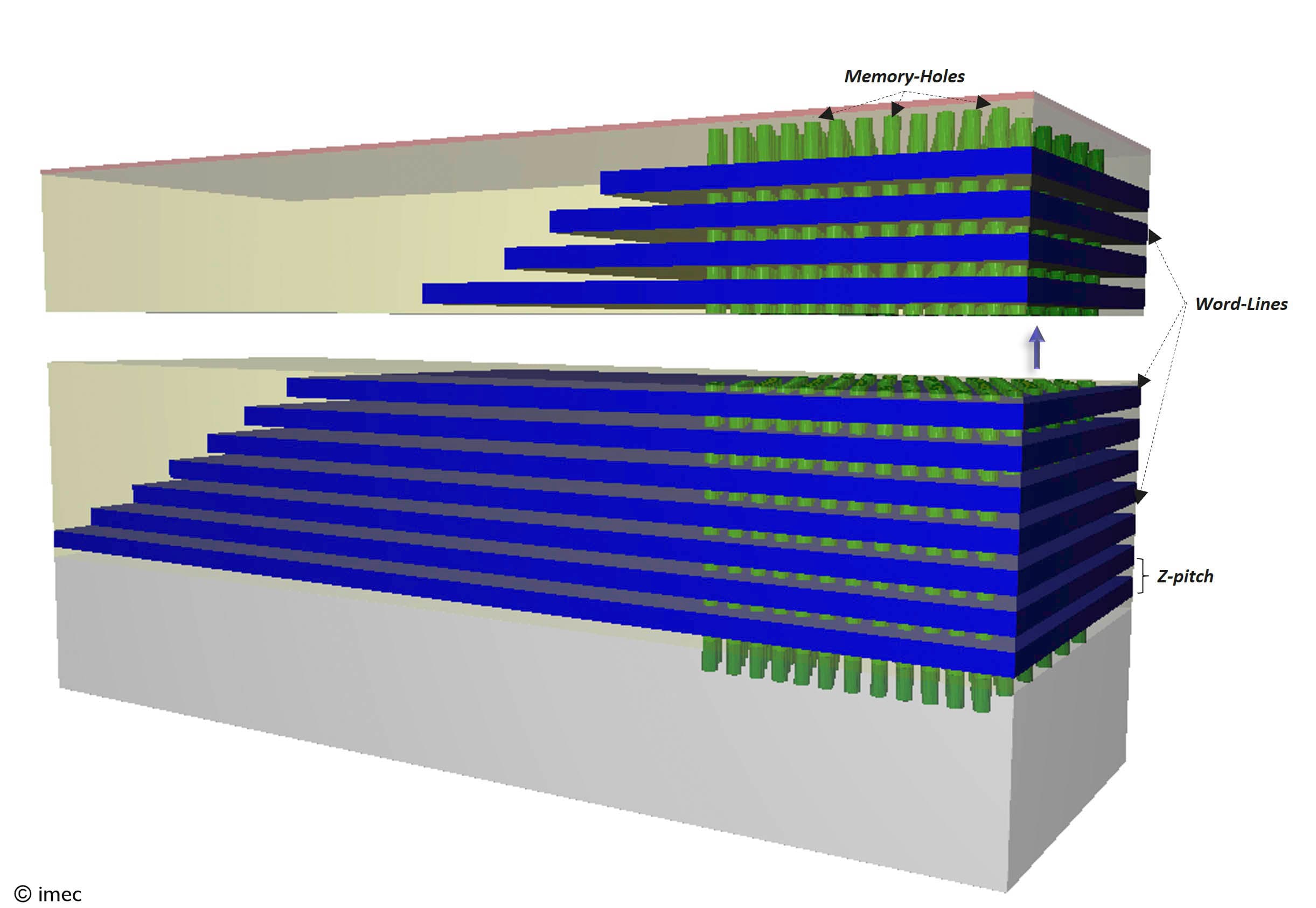
Z-pitch scaling of 3D NAND flash is of paramount importance to sustain the cost reduction of next-generation multi-layered GAA-based NAND flash. With z-pitch scaling, the pitch between adjacent word-lines – which today is about 40nm – is further reduced by scaling down the thickness of both word-line and Si-oxide layers in the stack. This allows adding more layers – and hence, memory cells – per ‘micrometer’ of stack height, providing a cost benefit.
Unfortunately, without optimizations, z-pitch scaling is experimentally observed to negatively impact the electrical performance of the memory cells. It results in threshold voltage reduction, enhanced sub-threshold swing, decreased retention, and increase of the program and erase voltages.
These effects can be assigned to two physical phenomena that become more dominant with further scaling: cell-to-cell interference and lateral charge migration.
When further reducing the thickness of the word-line layer, the gate length of the charge trap transistor shrinks accordingly. As a result, the gate increasingly loses control over the channel, facilitating electrostatic coupling between adjacent cells. In addition to cell-to-cell interference, the shrinking of the memory cells in the vertical direction leads to lateral charge migration (or vertical charge loss): charges trapped inside the SiN layer tend to migrate through the vertical SiN layer, compromising the retention.
Below, we discuss the technology enablers that can suppress these phenomena, allowing researchers to unlock z-pitch scaling for the next generations of 3D NAND flash.
Integrating airgaps in between word-lines for reduced cell-to-cell interference
TCAD simulations have shown that integrating an airgap in between neighboring word-lines is a promising way to suppress cell-to-cell interference. Airgaps have a lower dielectric constant than the Si-oxide inter-gate dielectric, reducing the electrostatic coupling between neighboring cells. It’s a ‘trick’ that worked very well in earlier planar 2D NAND flash architectures. But implementing airgaps in the tall Si-oxide/word-line stack is significantly more complicated. Solutions have been proposed [3] but have not proven to be fully scalable.
At the 2025 IEEE International Memory Workshop (IMW), imec presented a unique integration scheme that allows airgaps to form in a controllable way in between word-lines [4]. The integration scheme involves introducing the airgaps from within the memory-hole region, by recessing the inter-gate Si-oxide prior to depositing the ONO stack. The airgaps are introduced self-aligned to the word-line, allowing their positioning to be precisely controlled and providing a scalable solution.
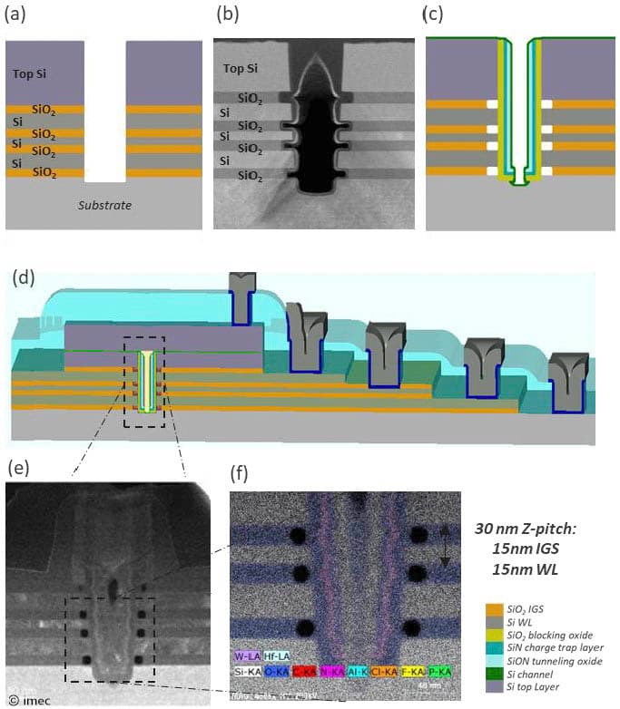
Devices with an airgap were shown to be less sensitive to neighboring cell interference than devices without airgap. This was concluded from the smaller shift in threshold voltage measured for devices with airgap when applying a so-called pass voltage on the unselected gates. The results were obtained on a test device with limited word-line layers at 30nm pitch (15nm gate length and 15nm Si-oxide inter-gate dielectric), and 80nm memory hole diameter. Imec researchers also investigated the impact of airgaps on memory performance and reliability. The airgaps did not affect the memory operation and showed an endurance of up to 1,000 program/erase cycles, comparable to devices without airgaps.
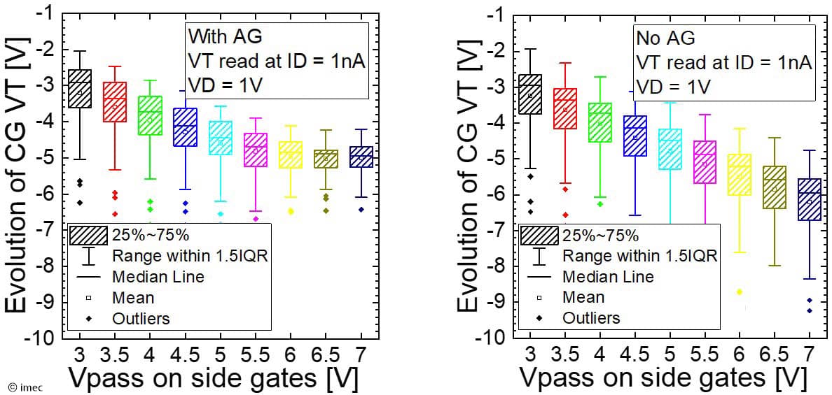
Based on these results, the hole-side airgap integration is considered a crucial step in enabling aggressive z-pitch scalability.
Introducing charge trap layer separation to suppress lateral charge migration
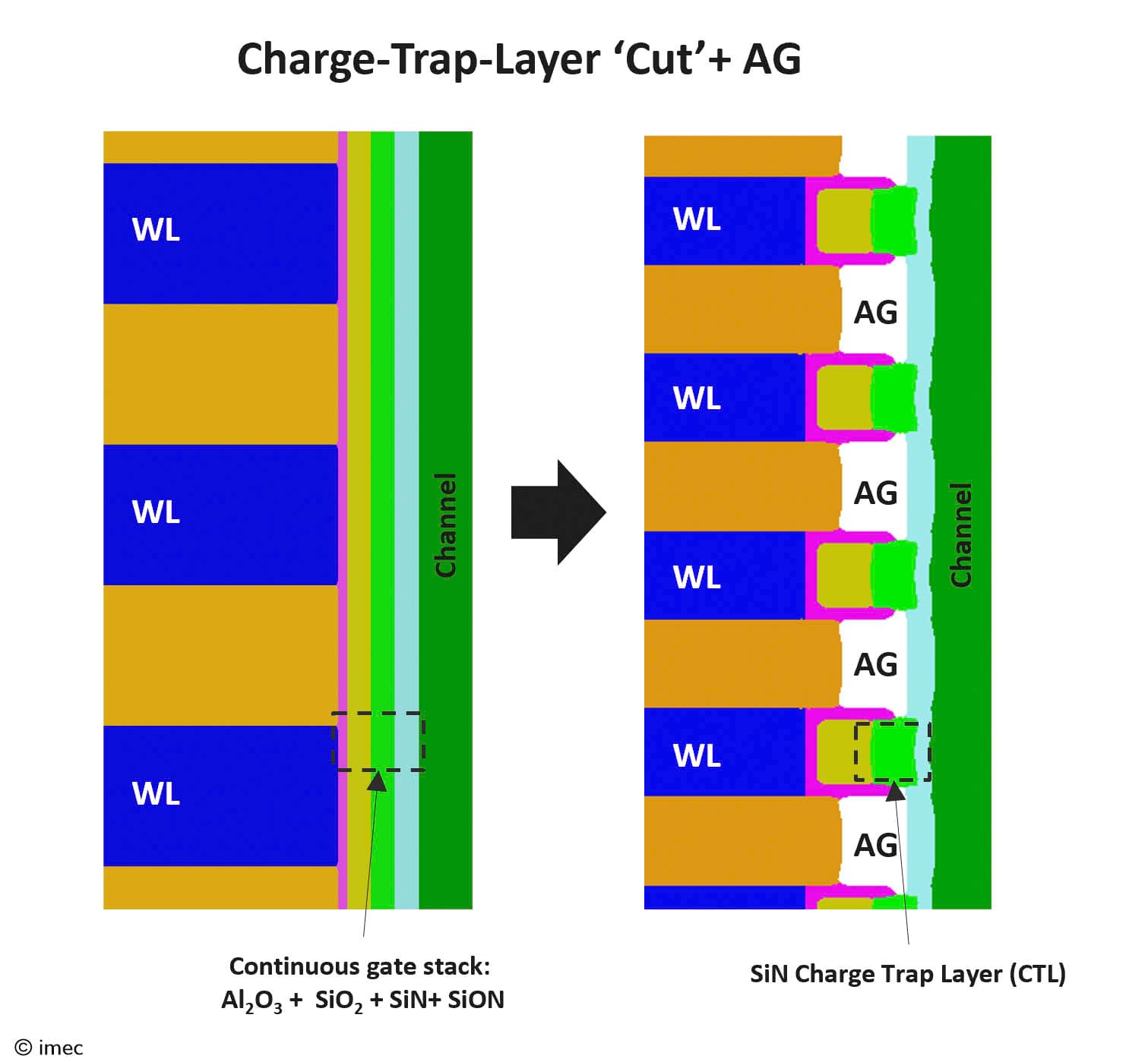
So far, imec has demonstrated the feasibility of introducing airgaps in the inter-gate dielectric layer, with airgaps ‘terminating’ at the location of the ONO stack’s blocking oxide. TCAD simulations show that further extending the airgap into the region of the blocking oxide and SiN charge trap layer would lead to an improved memory window. Such a charge trap layer separation (or charge trap cut) has an additional advantage: it would prevent charges trapped in the memory cell from migrating laterally through the SiN string that runs from top to bottom along the height of the oxide/word-line stack.
Implementing such a charge trap cut is, however, very challenging, as it requires directional etching and deposition through the sidewalls of extremely deep and narrow holes. For these structures, the toolbox of technologies available for planar 2D NAND flash is no longer applicable. Imec is currently working with its suppliers on new techniques that can enable this charge trap cut in a controllable way.
Once the charge trap layer can be successfully interrupted, imec researchers intend to combine it with the airgap integration scheme to provide a complete and scalable solution for the z-pitch scaling challenges.
Conclusion and outlook
Z-pitch scaling of GAA-based 3D NAND flash is critical for controlling the costs associated with the continued increase in word-line layers. Building on its long-standing processing expertise and strong ecosystem of equipment suppliers, imec is developing the key technologies that support aggressive z-pitch scaling while preserving memory operation and reliability: airgap integration and charge trap cut.
As the density increase of 3D NAND flash with GAA charge trap cell architecture will eventually saturate, research groups worldwide explore more disruptive cell architectures to continue the storage roadmap after 2030. In a recently proposed new 3D architecture, for example, the conduction channels of the memory cells are arranged horizontally instead of vertically [5]. In another approach, discussed by imec at 2023 IMW [6], charge trap memory cells are connected through a trench-based architecture instead of integrating the cells in a circular GAA geometry – offering a leap in bit storage density.
All these developments show that there are several technologies in the pipeline that will allow the memory industry to gradually move toward >100Gbit/mm2 of data storage – a demand driven primarily by cloud computing and AI applications.
This article was originally published in Electronic Design.
Want to know more?
[1] SK hynix Starts Mass Production of World's First 321-High NAND
[2] https://spectrum.ieee.org/flash-memory
[3] ‘A confined storage nitride 3D-NAND cell with WL airgap for cell-to-cell interference reduction and improved program performances’, D. Resnati, 2024 VLSI
[4] ‘Hole-side airgap integration as enabler for 3D NAND flash z-pitch scaling’, S. Rachidi et al., 2025 IEEE International Memory Workshop (IMW)
[5] ‘Superior scalability of advanced horizontal channel flash for future generations of 3D Flash memory’, M. Oda, 2024 IEDM
[6] ‘Imec improves memory window of a 3D trench cell for next-gen NAND Flash’, imec Reading Room
Authors

Sana Rachidi
Dr. Sana Rachidi received her M.Sc. degree in material science and surface treatments in 2016 from ENSIL-ENSCI Engineering school and from Limoges University, France. In 2020, she received her Ph.D. in nanoelectronics and nanotechnologies from Grenoble Alpes University UGA, France, where she worked on enabling dry and wet etch process developments for beyond 8nm GAA CMOS applications. She joined imec in Leuven, Belgium, in 2021 where she is currently working as a senior R&D engineer in memory process integration, semiconductor device design for multiple internal and external projects covering storage and MRAM applications

Maarten Rosmeulen
Maarten Rosmeulen received his M.Sc. degree in physics in 1993 and his M.Sc. degree in physics of micro-electronics and materials science in 1994, both from the KU Leuven, Belgium. In 2005, he received his Ph.D. in electrical engineering from the KU Leuven. Since then, he has been with imec, in Leuven, Belgium, where he has been active as an R&D engineer in process integration, semiconductor device design, and electrical device characterization for multiple internal and external projects. In 2009 he became a project leader in developing GaN-on-Silicon Light Emitting Diodes (LEDs). In 2014 he became the team leader of the Pixel Design and Testing team and has been responsible for the development of CMOS Image Sensor (CIS) technologies. In 2019 he became the program director of the Storage Memory program, the position he holds today.
Discover more
Imec achieves breakthroughs in ferroelectric memory research for next-generation memory solutions to meet AI-era data needs
Read more
Imec demonstrates the first 3D implementation of a charge coupled device for AI memory applications
Read more