The promise of OTS-only memories for next-gen compute system architectures

The discovery of a memory effect in ovonic threshold switching (OTS) devices paves the way to a new compute express link (CXL) memory

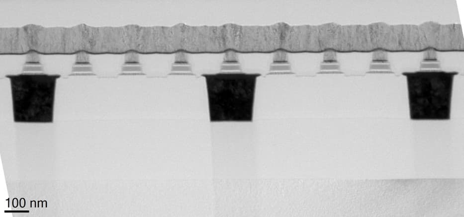
BlurHashMicroscope cross-section of a semiconductor structure with repeating narrow contacts and 100 nm scale bar

While investigating ovonic threshold switching (OTS) devices for selector applications, researchers at imec observed an interesting phenomenon: the device can operate as a memory itself.

This OTS-only memory involves a simple and cost-effective fabrication process, is scalable to larger densities, and shows promising performance characteristics for compute express link (CXL) memory-like applications – in between DRAM and NAND.

By reading this article, originally published in EDN, you will learn:

  •  how the OTS-only memory evolved out of OTS selector device technology,
  •  how it works,
  •  and which research directions are needed to meet the specs of a CXL memory for high-performance computing applications.

Read the article in EDN.

Authors

Portrait of Daniele Garbin standing indoors at imec with a blurred lab-like background

Daniele Garbin

R&D Engineer at imec
Author

Daniele Garbin received his Ph.D. in nanoelectronics and nanotechnology from Université Grenoble Alpes, Grenoble, France, in 2015. In 2016, he joined imec, Leuven, Belgium, where he works as an R&D Engineer. His current research interests include OTS and various emerging memory device technologies.

Read more about this author
Portrait of Gouri Sankar Kar standing in a bright hallway beside large windows

Gouri Sankar Kar

VP R&D compute & memory device technologies at imec
Author

Gouri Sankar Kar received the PhD degree in semiconductor device physics from the Indian Institute of Technology, Khragput, India in 2002. From 2002 to 2005, he was a visiting scientist at Max Planck Institute for Solid State Research, Stuttgart, Germany, where he worked with Nobel Laureate (1985, Quantum Hall Effect) Prof. Klaus von Klitzing on quantum dot FET. In 2006, he joined Infineon/Qimonda in Dresden, Germany as lead integration engineer. There he worked on the vertical transistor for DRAM application. In 2009, he joined imec, Leuven, Belgium, where he is currently ‎distinguished member of technical staff (DMTS). In this role, he defines the strategy and vision for RRAM, DRAM-MIMCAP and STT-MRAM programs both for stand-alone and embedded applications.
 

Read more about this author

Discover more

Researchers in cleanroom suits work at semiconductor equipment in a cleanroom

A technology platform for thermally stable DRAM peripheral transistors

20/05/2025
Page-turner
Memory & storage
CMOS: advanced & beyond
Read more
Glowing blue circuit traces radiate from a central microchip on a dark motherboard

Cross-technology co-optimization (XTCO)

Page
CMOS: advanced & beyond
Read more
Groene lichtpuntjes verspreid over horizontale lagen, als een abstract beeld van vloeistofgeheugen

Bringing SOT-MRAM technology closer to last-level cache memory specifications

16/12/2024
Research update
Memory & storage
CMOS: advanced & beyond
Read more
Blue abstract illustration of curved semiconductor wafer sections and chip-like patterns

White paper: monolithic microsystems

Page
Sensing and actuation
CMOS: advanced & beyond
Read more
Stylized 3D rendering of an imec research building at night with a glowing logo

Europe’s pilot line to enable future compute systems

21/10/2024
Vision
CMOS: advanced & beyond
NanoIC pilot line
Memory & storage
Read more
Gloved hands holding a printed chip layout with multiple die blocks

When does it make sense to move from a monolithic ASIC to a chiplet-based design?

23/06/2026
Longread
CMOS: advanced & beyond
Artificial intelligence
Read more
Cross-sectional micrograph of a ferroelectric memory device structure with a central dark pillar and 200 nm scale bar.

Imec achieves breakthroughs in ferroelectric memory research for next-generation memory solutions to meet AI-era data needs

17/06/2026
press release
Memory & storage
Read more
Cross-sectional micrograph of a chip structure with vertical interconnects and a 200 nm scale bar

Sony and imec unveil high-density backside connectivity module enabling next-generation 3D chip integration

16/06/2026
press release
CMOS: advanced & beyond
Read more
Groene lichtpuntjes verspreid over horizontale lagen, als een abstract beeld van vloeistofgeheugen

ASML, TSMC and imec bring industry-ready 2D-material transistors closer with breakthrough 300mm integration

15/06/2026
press release
CMOS: advanced & beyond
Read more

imec in your region

Looking for information about imec's activities in different parts of the world?

United Kingdom
United States
Qatar