Five good reasons, three major challenges for introducing 2D materials into logic
2D materials such as tungsten disulfide (WS2) can play a crucial role in the fabrication of future logic chips. Due to their exceptional properties, they promise to enable ultimate gate length scaling, and can therefore extend the logic transistor scaling roadmap. They could also revolutionize how we think about chip architecture, blurring the line between front-end and back-end by enabling compact back-end-compatible transistors.
In recent years, lab-based 2D-transistors have matured considerably, and a route is being developed for their industrial uptake. In parallel, remaining challenges towards improved device performance are being addressed.
Below, Iuliana Radu, program director at imec, explains the worldwide interest in these materials, especially their promise to further extend the logic technology roadmap.
1. 2D materials have remarkable properties
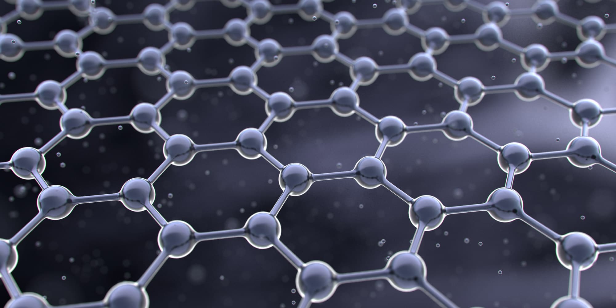
2D materials are a class of materials that form two-dimensional crystals. In this elegant 2D form factor, they have fascinating electrical, thermal, chemical and optical properties. The most famous of these materials is graphene, a hexagonal honeycomb shaped sheet of carbon atoms. Graphene has an outstanding mechanical strength, a large conductivity for both heat and electricity, and odd optical abilities.
But the exploration of 2D materials has moved far beyond graphene. The class of transition metal dichalcogenides, with chemical formula MX2, has versatile properties that complement those of graphene.
Unlike graphene, tungsten disulfide (WS2), molybdenum disulfide (MoS2) and a few others have a wide range of bandgaps, making them natural semiconductors. Depending on their chemical composition and structural configuration, atomically thin 2D materials can also be categorized as metallic or insulating. Thanks to their remarkable properties, opportunities for 2D materials have emerged in multiple application domains, including (bio)sensing, energy storage, photovoltaics, opto-electronics and transistor scaling [1, 2, 3].
2. 2D-based transistors promise ultimate gate length scaling
In chip manufacturing, 2D semiconductors such as WS2 and MoS2 have emerged as candidates to replace ‘good old Si’ in the conduction channel of the transistor. The great advantage? Compared to Si, 2D-based field-effect transistors (2D-FETs) promise to be more immune to short-channel effects – which have become a major hurdle for further Si-transistor scaling.
Indeed, as the Si-based transistor channel was made smaller and smaller, current started to leak across it even when there was no voltage on the gate. This effect, known as short-channel effect, became worse with each technology generation, jeopardizing further gate length scaling. The FinFET, today’s mainstream transistor technology, partly counters this effect. In this transistor architecture, the fin-shaped channel region can be made much thinner and the gate surrounds the channel on more than one side. This makes it easier for the gate voltage to control the flow of carriers inside the Si-based channel. The upcoming transition to the nanosheet transistor – with the gate now surrounding the channel on all sides – builds further on this idea, providing even better electrostatic control. However, when scaling beyond 3nm, these Si-based architectures will continue to suffer from unwanted short-channel effects.
And this is where high-mobility WS2 and MoS2 can come to the rescue. They can be structured in a few to even single atom layers, opening the possibility of providing very thin channel regions. This significantly restricts the pathway for the current to flow, making it harder for the charge carriers to leak away when the device is turned off. As such, they promise to enable ultimate gate length scaling (below 10nm), without worrying about short-channel effects.
In support of these promises, our team at imec recently performed a design-technology co-optimization (DTCO) study. We showed how 2D-FETs may further extend the logic device technology scaling roadmap, with stacked nanosheet transistor architectures as the most likely insertion point [4].
3. 2D materials may be used to build compact back-end-of-line switches
The application of 2D semiconductors may go beyond high-performance transistors. Another potential application area includes low-power circuits that have less performance and area restrictions. Examples are on-chip power management systems, signal buffers and memory selectors. On top of that, 2D materials might be used to revolutionize the chip’s back-end-of-line (BEOL), by enabling small back-end-compatible switches.
Chip fabrication can roughly be divided in two parts: the front-end-of-line (FEOL) where the transistors are built, and the BEOL where the transistors are linked through many layers of interconnects to form functional circuits and deliver power. With traditional transistor scaling becoming more and more challenging, scientists have been looking for ways to add transistors and small circuits in the BEOL – saving some area in the FEOL. But to do so, they can only use materials that can be integrated at relatively low temperatures – in order not to damage the devices and interconnects beneath them. This should be possible using 2D semiconductors. An additional advantage of using 2D-based transistors instead of some other ‘BEOL’ candidates is the potential ability to build n-type as well as p-type devices, a necessity in CMOS logic. This would allow the development of compact back-end logic CMOS circuits for power gating or as repeaters.
4. Lab-based ultra-scaled 2D transistors show great performance
But can we experimentally build these ultra-scaled 2D-FETs, and do they fulfill their promise in terms of performance? In recent years, scientists have explored a variety of MX2 materials. Initially, MoS2-based devices were shown to be the most mature, with highest experimental reported mobility values coming close to the theoretical value of 200cm2/Vs [5]. More recently, competitive results could be shown for WS2-based FETs as well – which theoretically have the higher performance potential. Progress was made towards improving contact resistance and enhancing device performance.
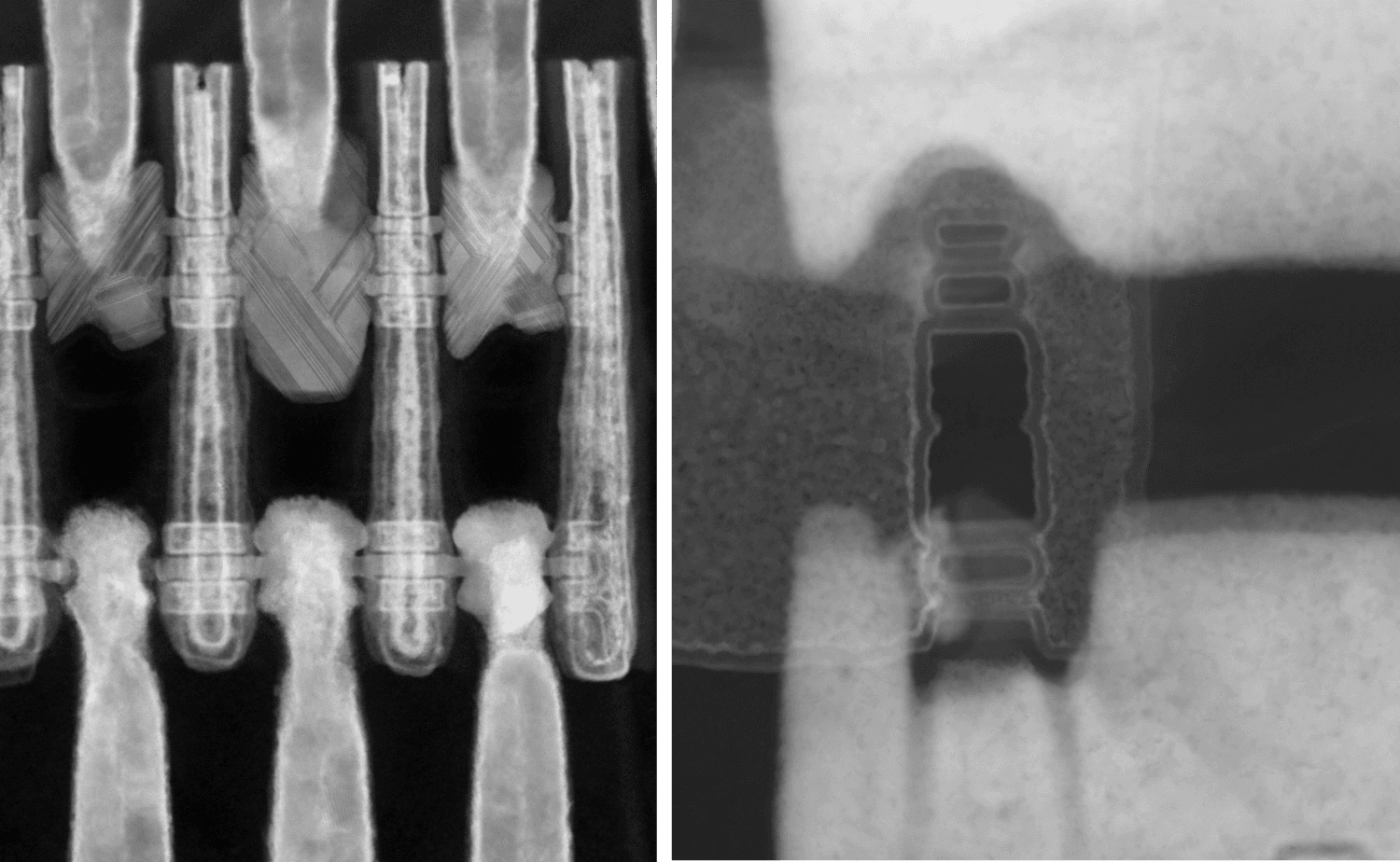
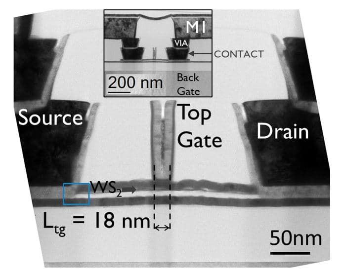
At imec for example, our team could demonstrate fully functional 2D-FETs with a channel of just 1-2 monolayers thickness and 30nm length. We also showed improved electrostatic control by using a dual-gated device structure. While traditional FETs have only one gate at the top, a dual-gate transistor has both a top and bottom gate, which, when connected, can improve the electrostatic control over the channel [4].
5. A route towards industrial-scale production of 2D-FETs is being developed
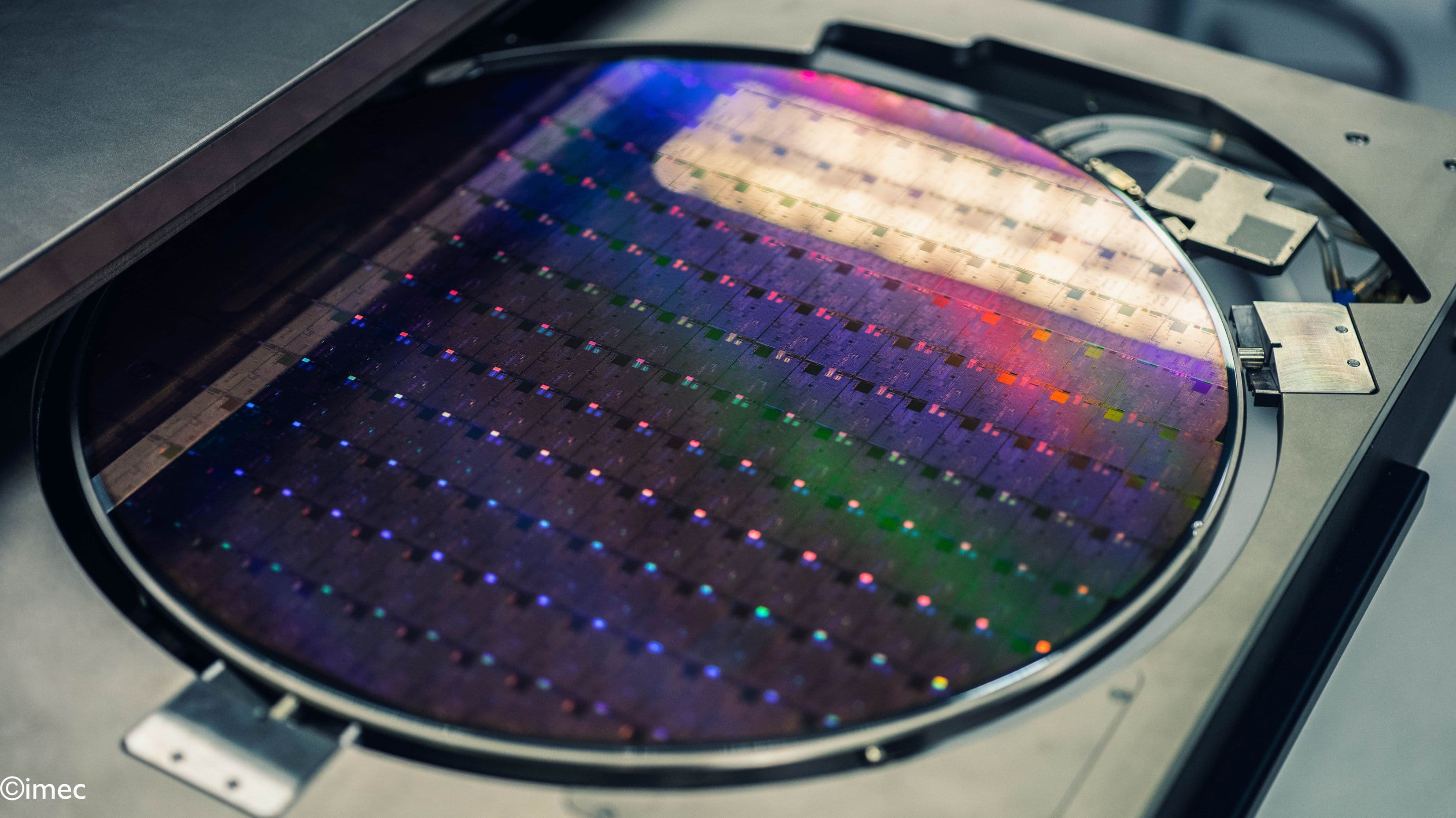
2D-FETs may only find their place in the logic technology roadmap if we can produce them in large volumes. That will be key for an industrial technology uptake. It means that we need to be able to get the devices out of the lab and integrate them on 300mm wafers – with industry-standard production tools.
Imec has set the scene for adopting these 2D materials into a 300mm integration flow. This flow is used to study the impact of various processing conditions and to work towards improved performance. High-quality growth of 2D materials on 300mm wafers could for example be demonstrated using metal-organic chemic vapor deposition (MOCVD) – a process that deposits crystals on a surface by means of a chemical reaction. With this tool, the thickness can be controlled with monolayer precision over the full 300mm wafer. Experiments showed the beneficial impact of a high deposition temperature (i.e., 950°C) on the layer’s crystallinity and defectivity [4].
More complex transistor architectures (such as stacked nanosheets or, further down the roadmap, complementary FETs (CFETs)) might however call for alternative deposition techniques. The same is true for processing back-end-of-line circuits that have a restricted thermal budget. Imec therefore investigates alternative deposition techniques and explores the feasibility of using a transfer process – allowing to move the 2D channel to an already partially fabricated 300mm Si substrate.
6. Three major challenges are being addressed
While for now, individual device performance is an order of magnitude lower than for reported lab devices, the 300mm integration flow is used to understand the process impact and to identify the integration roadblocks. The channel material quality and control of the defectivity remain the biggest challenge in improving device performance. A second roadblock is the contact resistance of the source/drain contacts that needs to be reduced to acceptable levels. Thirdly, comprehensive models need to be developed to enable the above-mentioned device architecture designs, with built-in realistic process assumptions.
The article was originally published in EDN.
Want to know more?
[1] Joint European effort to unlock the potential of graphene, imec reading room.
[2] Imec develops innovative graphene-silicon optical broadband modulator, imec press release.
[3] Graphene and two-dimensional materials for silicon technology, D. Akinwande et al., Nature volume 573, pages 507–518 (2019).
[4] Imec introduces 2D materials in the logic device scaling roadmap, imec reading room.
[5] Intrinsic electrical transport and performance projections of synthetic monolayer MoS2 devices, K.K.H. Smithe et al, 2D Materials 4, 011009 (2017).
Authors

Iuliana Radu
Iuliana Radu is program director at imec, where she is leading the beyond CMOS and quantum computing activities. Prior to joining the logic program at imec in 2013, she was a Marie Curie and FWO fellow at KU Leuven and imec. Her work at imec and KU Leuven includes devices using the metal-to-insulator transition, ionic and electronic transport in functional oxides and devices with graphene and other 2D materials. Iuliana has received a PhD in physics from MIT in 2009 where she worked on the fractional quantum Hall effect and searched for non-abelian quasiparticles.
Discover more