Imec introduces 2D materials in the logic device scaling roadmap
Introduction is backboned by pathfinding work on 300mm integration and insights in device variability


In short
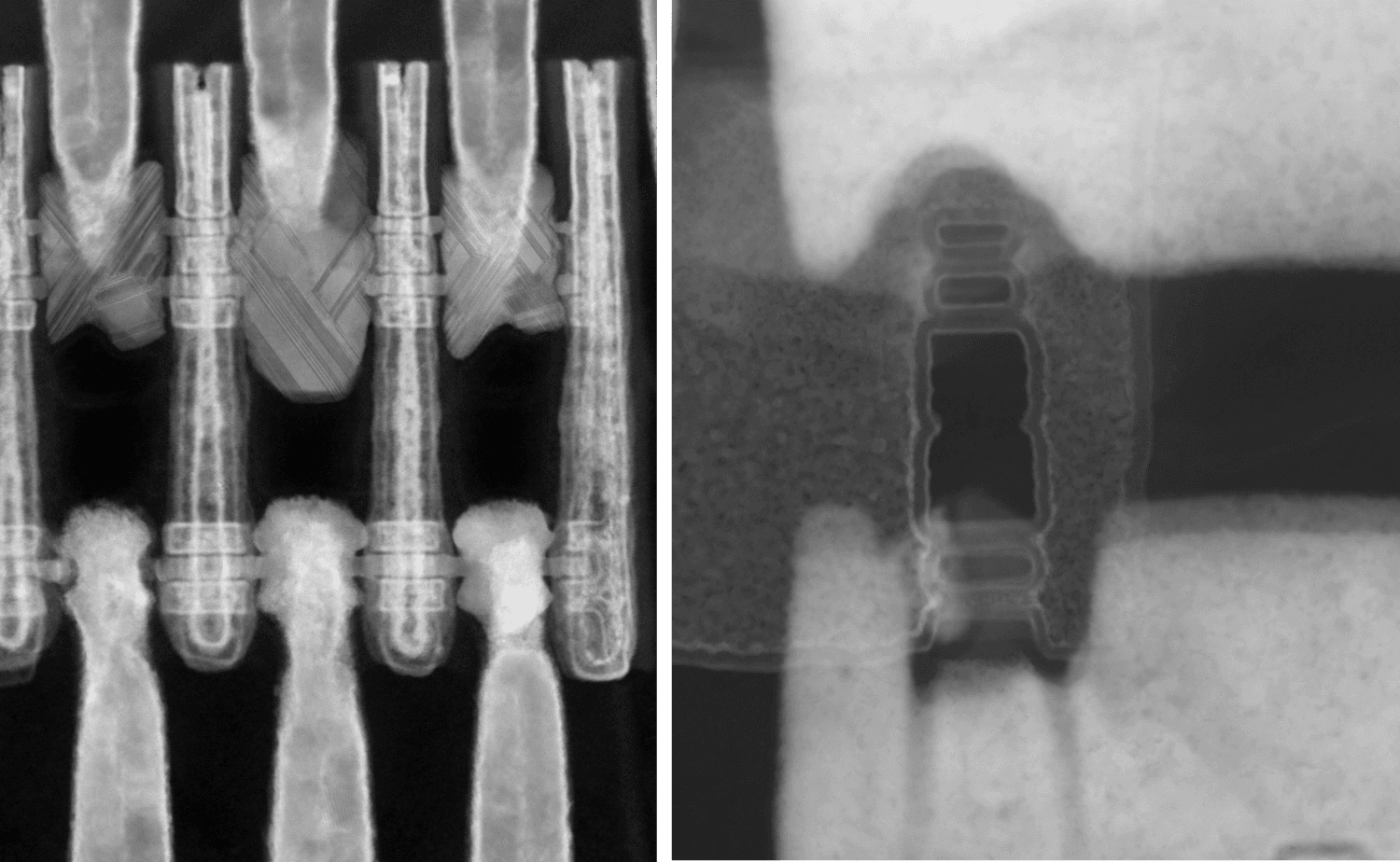
At the 2020 IEDM conference, imec proposes that 2D semiconductors like tungsten disulfide (WS2) can further extend the logic transistor scaling roadmap. The team laid the groundwork for integrating 2D semiconductors in a 300mm CMOS fab, and worked towards improved device performance. These findings are presented in four IEDM papers, one of which was selected as IEDM highlight.
The promise of 2D materials for high-performance applications
The continual scaling of Si-based transistors is challenged by short channel effects that limit further gate length scaling. Field-effect transistors (FETs) with semiconducting transition metal dichalcogenides (MX2, such as WS2 or MoS2) as the semiconductor channel promise however to be relatively immune to these short channel effects. FETs with 2D semiconductor channel owe this promise to the ability to make atomically thin channels combined with the theoretical ability to maintain higher carrier mobility – independent of channel thickness. These two properties give the gate voltage a better electrostatic control over the channel. Iuliana Radu, program director at imec: “2D-FETs are considered prime candidates to further extend the logic device scaling roadmap. Our team at imec has set the scene for adopting these 2D semiconductors into a 300mm integration flow – a key requirement for industrial adoption. We also obtained significant steps forward in improving device performance and in building fundamental understanding.”
Extending the logic device scaling roadmap with 2D-FETs: a DTCO analysis
“By using our design-technology co-optimization (DTCO) framework, we show how transistors with 2D semiconductor channel can further extend the logic scaling roadmap,” says Zubair Ahmed, imec researcher and first author of the paper on DTCO [1]. “A circuit-level power-performance-area (PPA) evaluation at 2nm revealed for example that devices in a stacked 2D-nanosheet configuration outperform their Si-based counterparts and have a reduced footprint.” Within the model, the team used realistic assumptions as much as possible based on experimental data.
A 300mm platform for dual-gated 2D-FETs
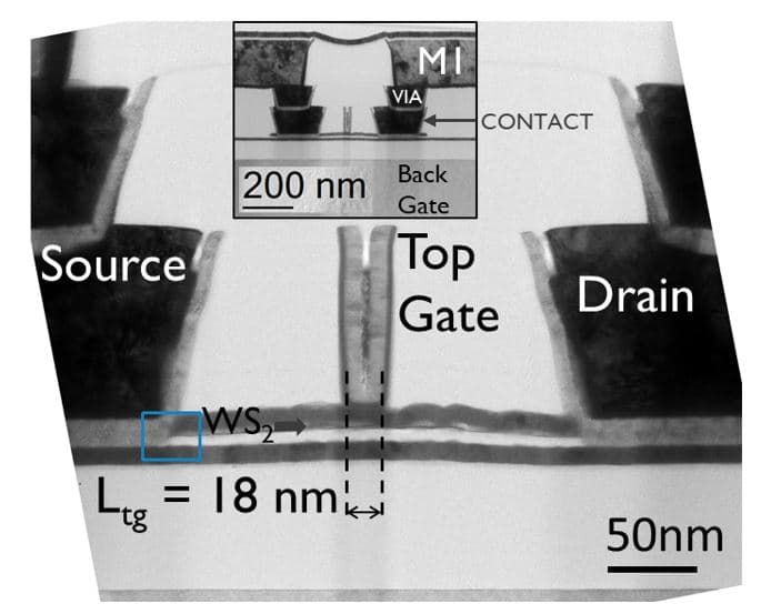
Several years ago, imec started pathfinding work on 300mm integration of both WS2- and MoS2-FET devices – a key requirement for industrial adoption. Inge Asselberghs, program manager of Exploratory Logic at imec and first author of the paper on 300mm integration [2]: “This work has resulted in a unique 300mm test vehicle for 2D-FETs, allowing the fabrication of functioning devices with gate lengths down to 18nm. The flow was used to study the impact of various processing conditions, such as the channel deposition and transfer process.” The team also identified remaining challenges, including 2D growth quality, formation of the gate dielectric, doping and contact resistance.
In the above-mentioned work, a dual-gated device structure was implemented. This is an important enabler for improved electrostatic control. “We showed experimentally that 2D-FETs with connected top and back gate outperform single-gate counterparts in terms of drive current, transconductance and sub-threshold swing – important metrics for evaluating short-channel effects,” explains Dennis Lin, principle scientist at imec and first author of the paper on dual-gated 2D-FETs [3]. The dual-gate concept also shows promise towards complementary MOS (CMOS) operation.
Sources of variability
The integration and device performance work were complemented with the first-ever variability study of a large set of nanoscale 2D-FET devices. The team investigated various sources of variability – including the thickness of the 2D-channel, the presence of bilayer islands and the 2D growth template – and their respective impact on the electrical performance (mainly on the subthreshold regime). Quentin Smets, senior researcher at imec and first author of the ‘variability’ paper [4]: “As a main conclusion, we found that variability can be strongly reduced if we thin down the 2D-based channel to a single uniform monolayer. This is an encouraging result, as very thin channels will be needed for further transistor scaling.”
Want to know more?
More details can be found in 4 papers presented at the 2020 IEDM conference:
- [1] ‘Introducing 2D-FETs in device scaling roadmap using DTCO’, Z. Ahmed et al.
- [2] ‘Wafer-scale integration of double gated WS2-transistors in 300mm Si CMOS fab’, I. Asselberghs et al.
- [3] ‘Dual gate synthetic WS2 MOSFETs with 120µS/µm Gm 2.7µF/cm2 capacitance and ambipolar channel’, D. Lin et al.
- [4] ‘Sources of variability in scaled MoS2 FETs’, Q. Smets et al. (IEDM highlight paper)
Authors

Iuliana Radu
Iuliana Radu is program director at imec, where she is leading the beyond CMOS and quantum computing activities. Prior to joining the logic program at imec in 2013, she was a Marie Curie and FWO fellow at KU Leuven and imec. Her work at imec and KU Leuven includes devices using the metal-to-insulator transition, ionic and electronic transport in functional oxides and devices with graphene and other 2D materials. Iuliana has received a PhD in physics from MIT in 2009 where she worked on the fractional quantum Hall effect and searched for non-abelian quasiparticles.
Zubair Ahmed
Researcher at imec working on DTCO for transistors with 2D semiconductor channel.
Dennis Lin
Principal Scientist at imec, leading work on devices with 2D semiconductors
Quentin Smets
Senior Researcher at imec working on transistors with alternative channel materials.
Discover more