Five semiconductor-based concepts that will revolutionize DNA sequencing
Cross-fertilization between disciplines has proven to be the secret ingredient for many great innovations. What if we would merge the semiconductor and the sequencing world?

In short
Interdisciplinary research and the recruitment of new expertise will be indispensable to fuel the next era in genomics.
Semiconductor technology and new CMOS-based concepts are good candidates to deliver such new expertise. As no other, the semiconductor industry has succeeded in making more complex and scalable systems, in compact form factors and at reduced prices, with improvements year after year.
1. Cross-layer optimization for better deep-sequencing and point-of-care systems
There was a time in semiconductor history when scaling was fun (i.e. making transistors smaller was rewarded by more performant and power-efficient circuits) and scientists didn’t have to leave their lab (i.e. everyone was specialized in a specific niche and didn’t need to interact with colleagues from other disciplines). Early 2000, this path of ‘happy scaling’ came to a halt and new tricks were needed to provide consumers with ever better computers, smartphones en other electronic devices.
“The semiconductor industry learned to take a new, wider view on its systems,” explains Liesbet Lagae, imec Fellow and Program Director Life Science Technologies. “When designers and technology experts talked to each other, the design could be made smarter, incorporating the pros and cons of new and older transistor technologies. The concept of cross-layer optimization came on scene as a new way to further improve systems in cost and complexity.”
The genomics industry has also experienced its ‘happy scaling’ era with a more than million-fold decrease in cost per genome. Liesbet Lagae: “We, at imec, believe that new expertise such as semiconductor process technologies and semiconductor-based concepts can enable the continuation of this path, towards 100 and even 10 dollar per genome. The concept of cross-layer optimization will be very important in this context: taking a more holistic view on the system and optimizing the system layers in relation to the other layers of the system. Think of layers such as materials, components, circuits, system hardware, system software, ...“
2. Micro-structures in silicon for an automated sample prep
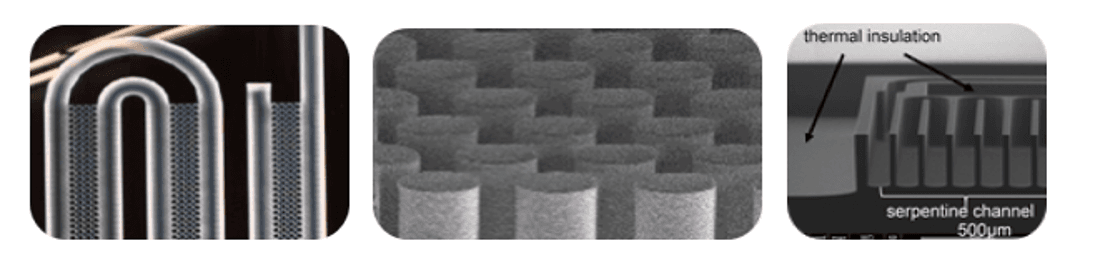
Today, sample preparation for sequencing requires different instruments equipped by skilled operators. This results in a lot of queuing time and a high turnaround time. The solution to this problem is a full automation of these preparation steps. A promising route to achieve this is by using smart precision microfluidic channels, structures, and concepts, both for deep sequencing and point-of-care sequencing. Part of these structures can be made of plastic, which is the standard material in current solutions, while other structures can be made in glass or silicon. The latter materials have the advantage that very small structures can be made with extremely precise technologies such as lithography.
“Indeed, lithography is a technology that is responsible for the success of the semiconductor industry,” explains Liesbet Lagae. “It can be used to define very precise and ultrasmall structures to make up the microfluidics part of a sequencing solution. Although more expensive than current techniques, it is extremely interesting to make hundreds or thousands of structures to work simultaneously or when precise features and sensors are needed to increase accuracy. Small structures also translate into small and well-defined volumes of reagents and sample, and faster chemical reactions. Moreover, the semiconductor precision manufacturing capabilities enable entirely new functions driven by microfeatures such as micro-pillar mediated filters, sieves or extraction devices. Realizing the sample-preparation flow with a semiconductor process has an extra advantage, i.e. a high degree of integration of all the components needed for a smart preparation flow. This is especially interesting for point-of-care devices with a limited form factor. One single integrated solution can e.g. comprise pumps and valves, sensors, microscopes, dielectrophoretic capture devices and microprocessors for data processing.”
3. Multi-electrode chips for spatial omics
A new emerging field in sequencing is single-cell sequencing. It’s a high-resolution next-generation sequencing method that allows to detect cellular differences in DNA/RNA code. This can be interesting to find mutations between different cancer cells, to study the function of different cell types, or to gain insight in the adaptability of microbial systems.
When all this is done while also having spatial information on these cells (i.e. where in the tissue the cell is located), it’s termed spatial genomics or spatial omics.
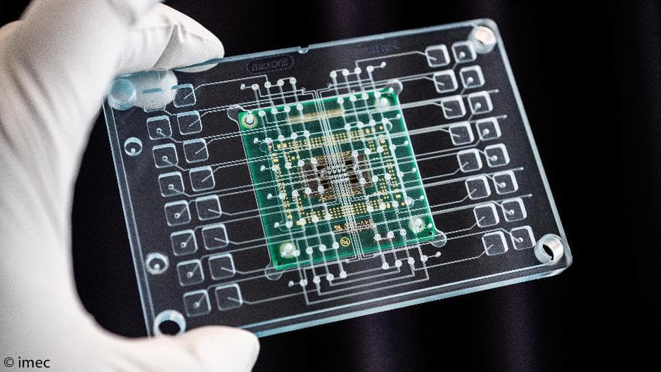
A promising tool to execute spatial omics is a multi-electrode (MEA) chip, like the one the imec is developing (see press release 2018). Liesbet Lagae: “Thanks to semiconductor manufacturing technologies, it’s possible to make thousands of small micrometer-sized electrodes that each are individually addressable by the underlying electronics. By applying voltages, individual cells can be stimulated or measured. Imagine a tissue or tumor biopsy placed on top of the MEA chip, with each electrode carrying a place tag that can be incorporated in the cells through electroporation. Next, the cells can be sequenced and via data analysis and the location tag the genetic heterogeneity in the tissue can be digitally reconstructed and overlayed with conventional pathological microscopic information.”
4. Fan-out wafer level packaging for next-gen assembly and integration
With the different layers in place - readout electronics, sensor array, photonic components and microfluidic structures – the flow cell is finalized by fabricating a cartridge with in- and outlets to allow interaction with the outside world. This includes electrical and photonic signals and fluid ins and outs.
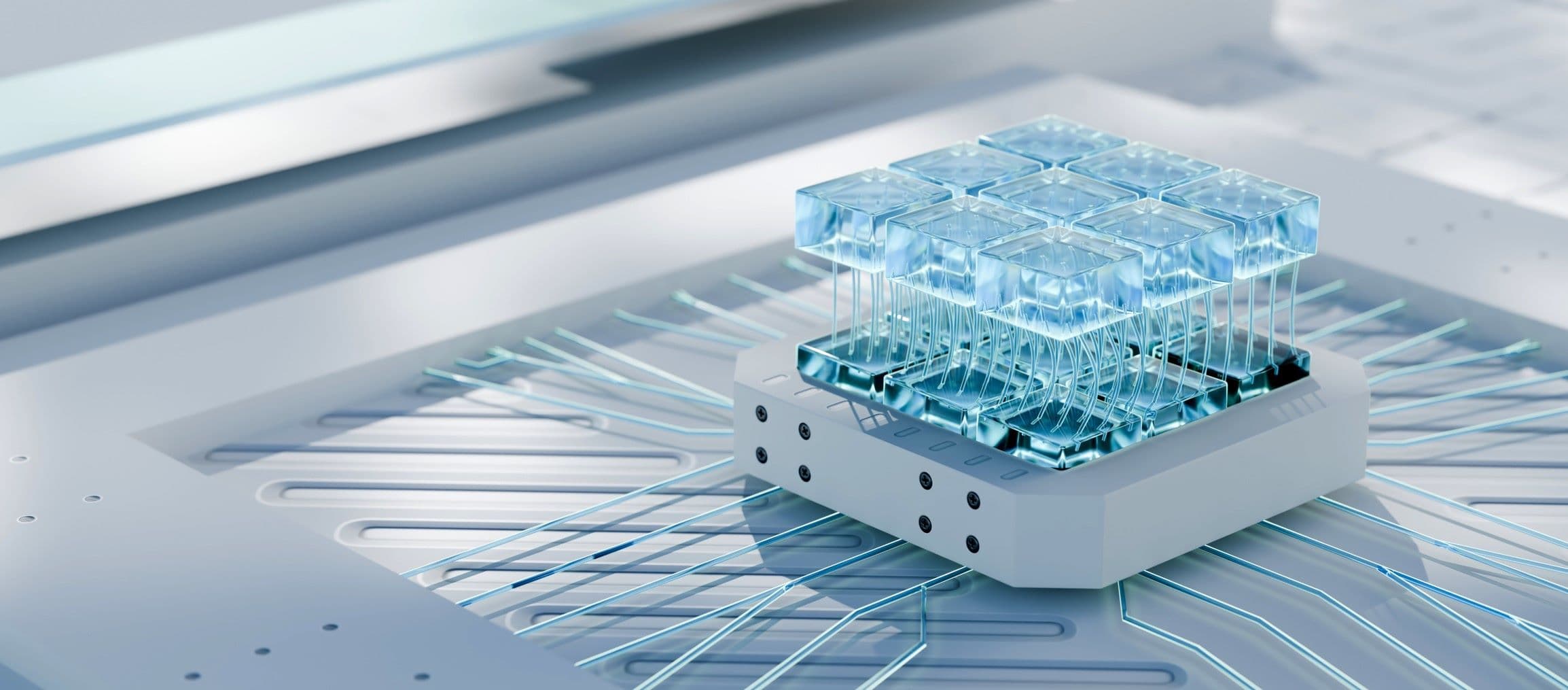
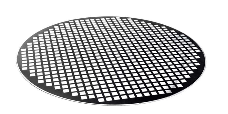
There is not yet a standard sensor/microfluidic/cartridge integration solution available like for semiconductor chips. So, for every application a dedicated platform choice needs to be made. Three main packaging solutions exist, each with specific pros and cons. “The one we want to highlight here, is know in the semiconductor world but not yet in the sequencing domain,” explains Liesbet Lagae. “In the fan-out wafer-level packaging technique, the chip wafer is diced into individual dies which are then placed on a new ‘reconstructed’ wafer with more spacing in between the dies. Afterwards, additional microfluidics (e.g. cartridge) can be placed on top in a wafer-level style. The technique can also be used to connect multiple silicon dies, e.g. sample prep precision fluidics with sequencing sensor dies. The technique combines cost benefits (because of a high manufacturing volume) with a good resolution and dimensional flexibility.”
5. Privacy-preserving AI for population genomics
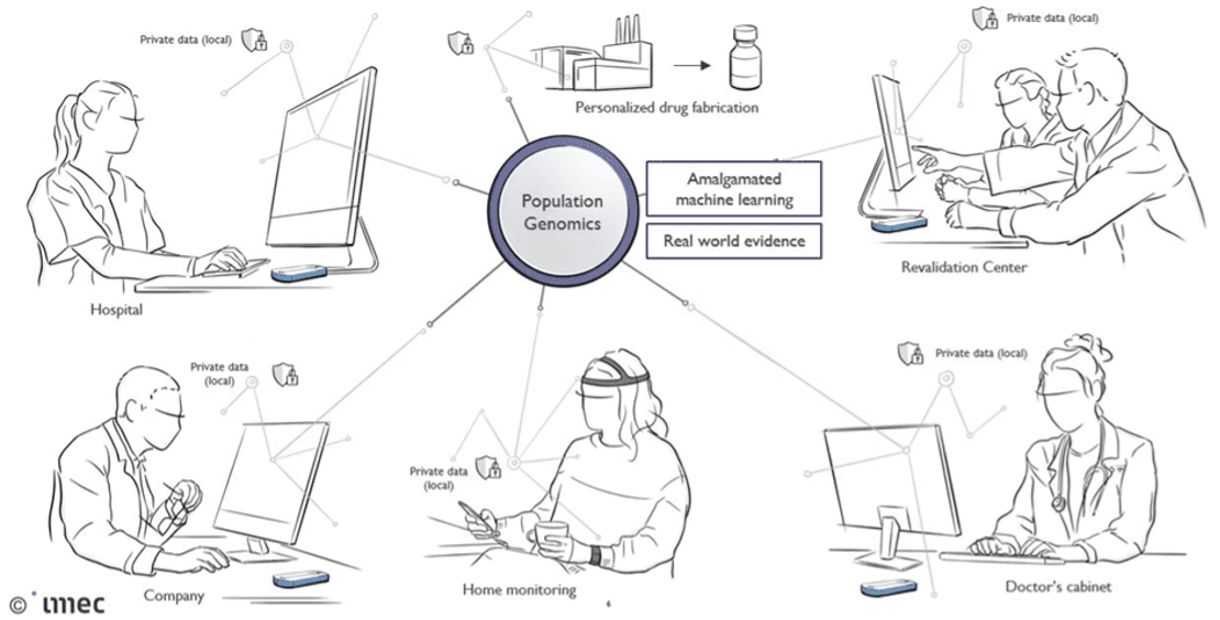
Personalized medicine is based on population genomics, i.e. the comparison of the genomics data of millions of people to better understand health and diseases. In daily clinical practice this would mean that the DNA and patient history of a specific person is compared to the rest of the world to get answers e.g. about the type of cancer of the patient and about the best treatment.
An important hurdle in unleashing the enormous power of population genomics, is the privacy of health data and the fact that health info is split and owned by all kinds of entities: hospitals, health insurers, pharma companies, wearable companies such as Fitbit, Google, Apple, ....
Liesbet Lagae: “The solution is amalgamated machine learning. It enables population genomics across genome centers and hospitals, while preserving privacy of data and models. These privacy-preserving machine-learning algorithms can access, manage, and exchange data insights across platforms and across owners without releasing sensitive information about the internal data, nor about the models of those who own it.”
Want to know more?
- Download the white paper ‘Semiconductor technologies and system concepts to revolutionize genomics’ via this link.
Authors

Liesbet Lagae
Liesbet Lagae is imec Fellow and co-founder and Program Director of the Life Science Technologies in imec. In this role, she oversees the emerging R&D, the public funded activities and early business creation. She holds a PhD degree from the KU Leuven, Belgium for her work on Magnetic Random Access Memories. As a young group leader, she has initiated the field of molecular and cellular biochips leveraging silicon technologies at imec, Belgium. The life science program has grown from emerging activities to a mature business line that provides smart silicon chip solutions to the life science industry. Applications include medical diagnostics, point-of-care solutions, DNA sequencing, cytometry, bioreactors, neuroprobes, implants. She holds a prestigious ERC consolidator grant for developing a platform on single cell analysis and sorting. She has (co-) authored 125 peer-reviewed papers in international journals and holds 15 patents in the field. She is also part-time professor in nanobiotechnology at KU Leuven/Physics department.
Discover more