Imec Reports First Electrical Demonstration of Integrated Forksheet Devices to extend Nanosheets beyond 2nm technology node
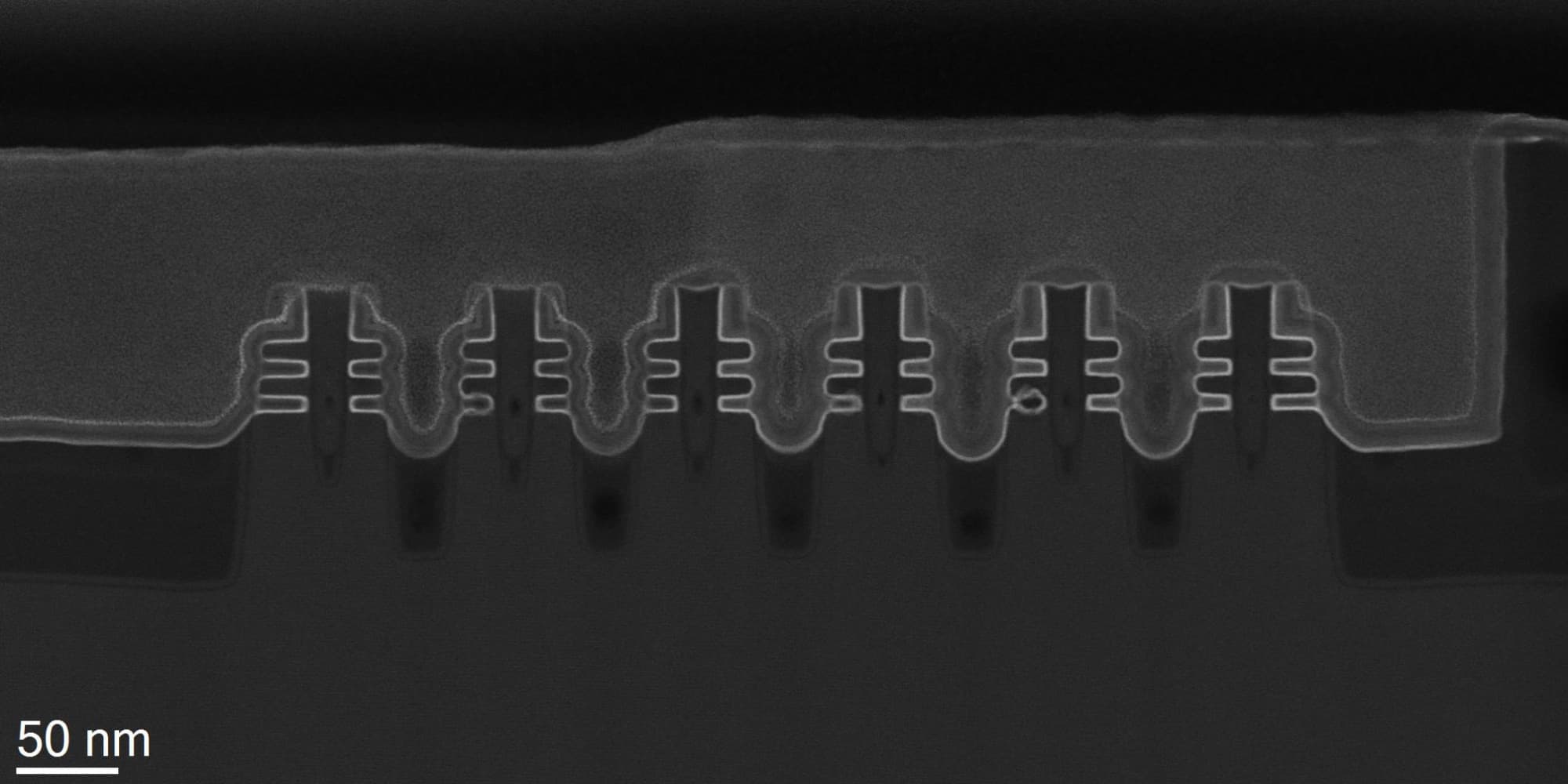
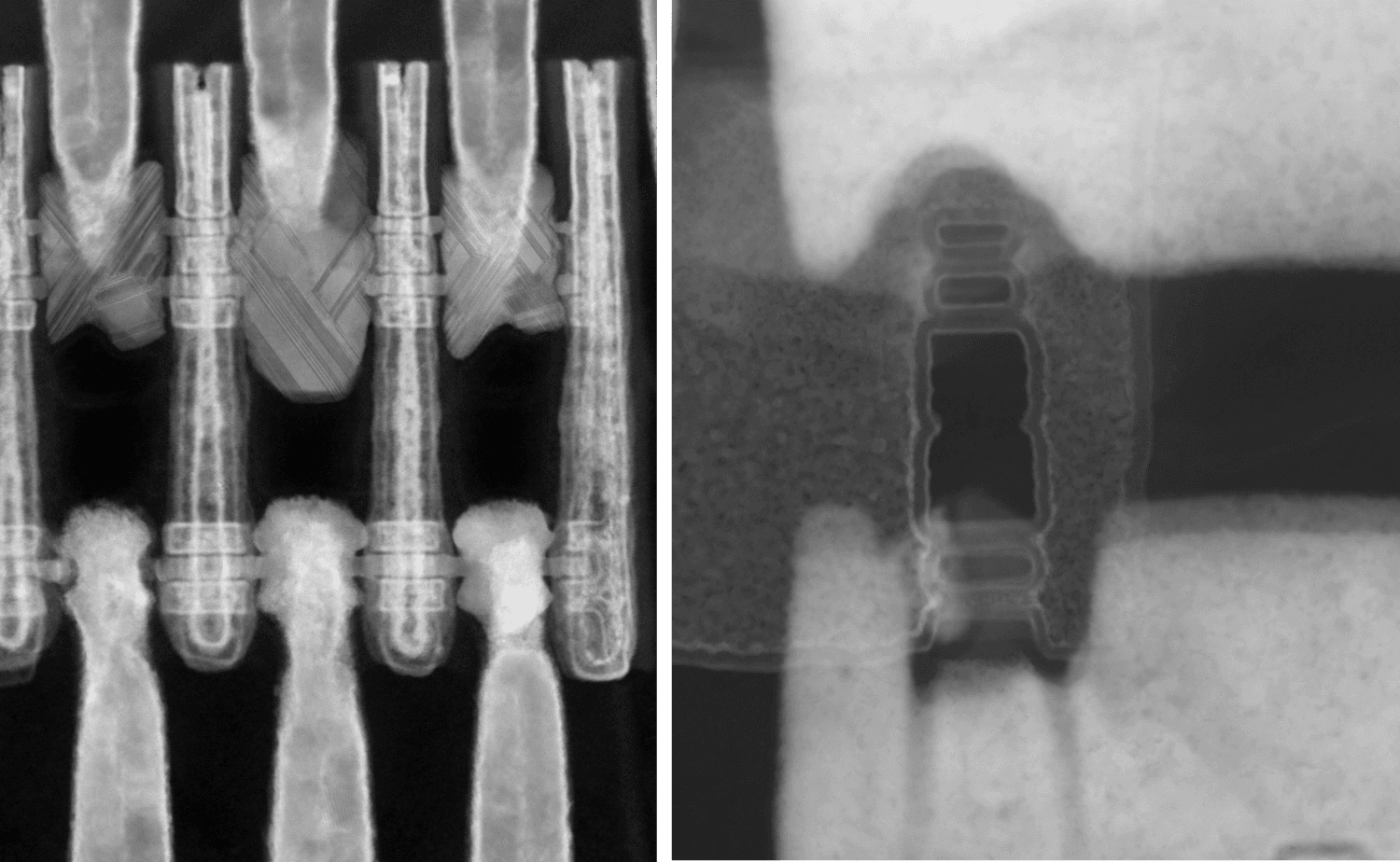
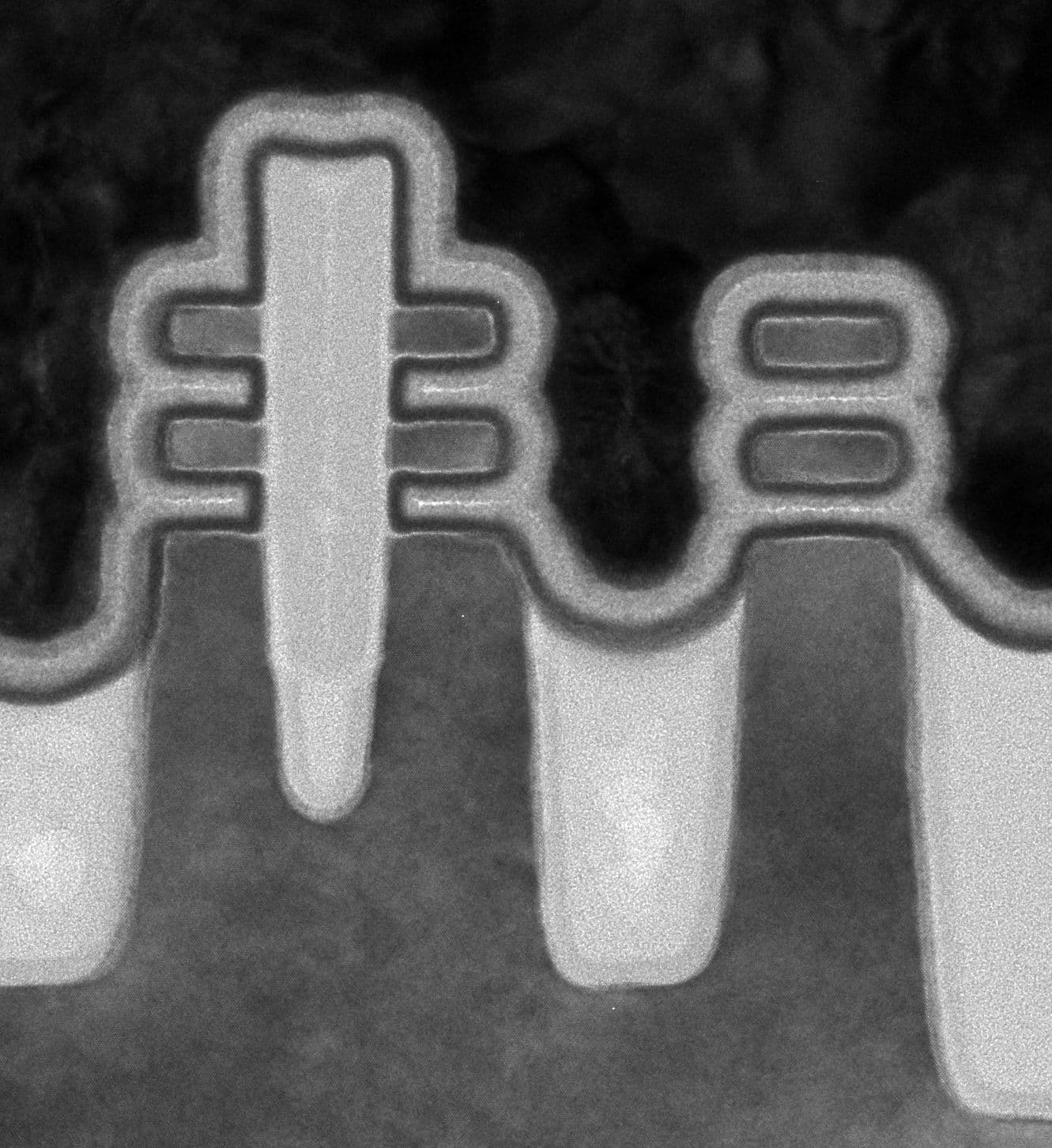
LEUVEN (Belgium), JUNE 15, 2021 — This week, at the 2021 Symposia on VLSI Technology and Circuits (VLSI 2021), imec, a world-leading research and innovation hub in nanoelectronics and digital technologies, demonstrates for the first time fully functional integrated forksheet field-effect transistors (FETs), with short-channel control (SSSAT=66-68mV/dec) comparable to gate-all-around (GAA) nanosheet devices down to 22nm gate length. Dual work function metal gates are integrated at 17nm spacing between n- and pFETs, highlighting the key benefit of forksheet devices for advanced CMOS area scaling.
The forksheet device has recently been proposed by imec as the most promising device architecture to extend the GAA nanosheet device generation with additional scaling and performance beyond 2nm technology node. Unlike nanosheet devices, the sheets are now controlled by a tri-gate forked structure – realized by introducing a dielectric wall in between the p- and nMOS devices before gate patterning. This wall physically isolates the p-gate trench from the n-gate trench, allowing a much tighter n-to-p spacing than what is possible with either FinFET or nanosheet devices. Technology assessment based on TCAD simulations earlier showed superior area and performance scalability. The performance increase is mainly attributed to a reduced Miller capacitance – resulting from a smaller gate-drain overlap.
Imec presents for the first time an electrical characterization of its forksheet devices that were successfully integrated by using a 300mm process flow, with gate lengths down to 22nm. Both n- and pFETs, each with two stacked Si channels, were found to be fully functional. Their short channel control (SSSAT = 66-68mV) was comparable to that of vertically stacked nanosheet devices that were co-integrated on the same wafer. For the forksheet devices, dual work function metal gates were integrated using a replacement metal gate flow at an n-p space as tight as 17nm (which is about 35% of the spacing in state-of-the-art FinFET technology), highlighting one of the key benefits of the new device architecture.
“From 2022 onwards, it is expected that today’s leading-edge FinFET transistors will gradually give way to vertically stacked nanosheet transistors in high-volume manufacturing, as the FinFET fails to provide enough performance at scaled dimensions,” explains Naoto Horiguchi, Director CMOS Device Technology at imec. “Process limitations will however pose a limit to how close the nanosheet’s n and p devices can be brought together, challenging further cell height reduction. The new forksheet device architecture – which is a natural evolution of the GAA nanosheet device – promises to push this limit, allowing track height scaling from 5T to 4.3T while still offering a performance gain. Alternatively, with a forksheet design, the available space can be used to increase the sheet width and as such further enhance the drive current. Our electrical characterization results confirm that the forksheet is the most promising device architecture to extend the logic and SRAM scaling roadmaps beyond 2nm leveraging the nanosheet integration in a non-disruptive way.”
About imec
Imec is a world-leading research and innovation center in nanoelectronics and digital technologies. Imec leverages its state-of-the-art R&D infrastructure and its team of more than 4,500 employees and top researchers, for R&D in advanced semiconductor and system scaling, silicon photonics, artificial intelligence, beyond 5G communications and sensing technologies, and in application domains such as health and life sciences, mobility, industry 4.0, agrofood, smart cities, sustainable energy, education, … Imec unites world-industry leaders across the semiconductor value chain, Flanders-based and international tech, pharma, medical and ICT companies, start-ups, and academia and knowledge centers. Imec is headquartered in Leuven (Belgium), and has research sites across Belgium, in the Netherlands, Taiwan and the USA, and offices in China, India and Japan. In 2020, imec's revenue (P&L) totaled 680 million euro.
Further information on imec can be found at www.imec-int.com.
Imec is a registered trademark for the activities of imec International (IMEC International, a legal entity set up under Belgian law as a “stichting van openbaar nut”), imec Belgium (IMEC vzw supported by the Flemish Government), imec the Netherlands (Stichting IMEC Nederland), imec Taiwan (IMEC Taiwan Co.), imec China (IMEC Microelectronics (Shanghai) Co. Ltd.), imec India (IMEC India Private Limited), imec San Francisco (IMEC Inc.) and imec Florida (IMEC USA Nanoelectronics Design Center Inc.).
Discover more