Imec Ramps Up the Development of the High-NA EUV Patterning Ecosystem
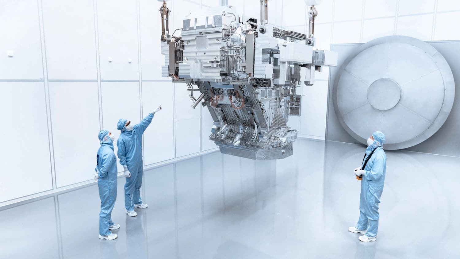
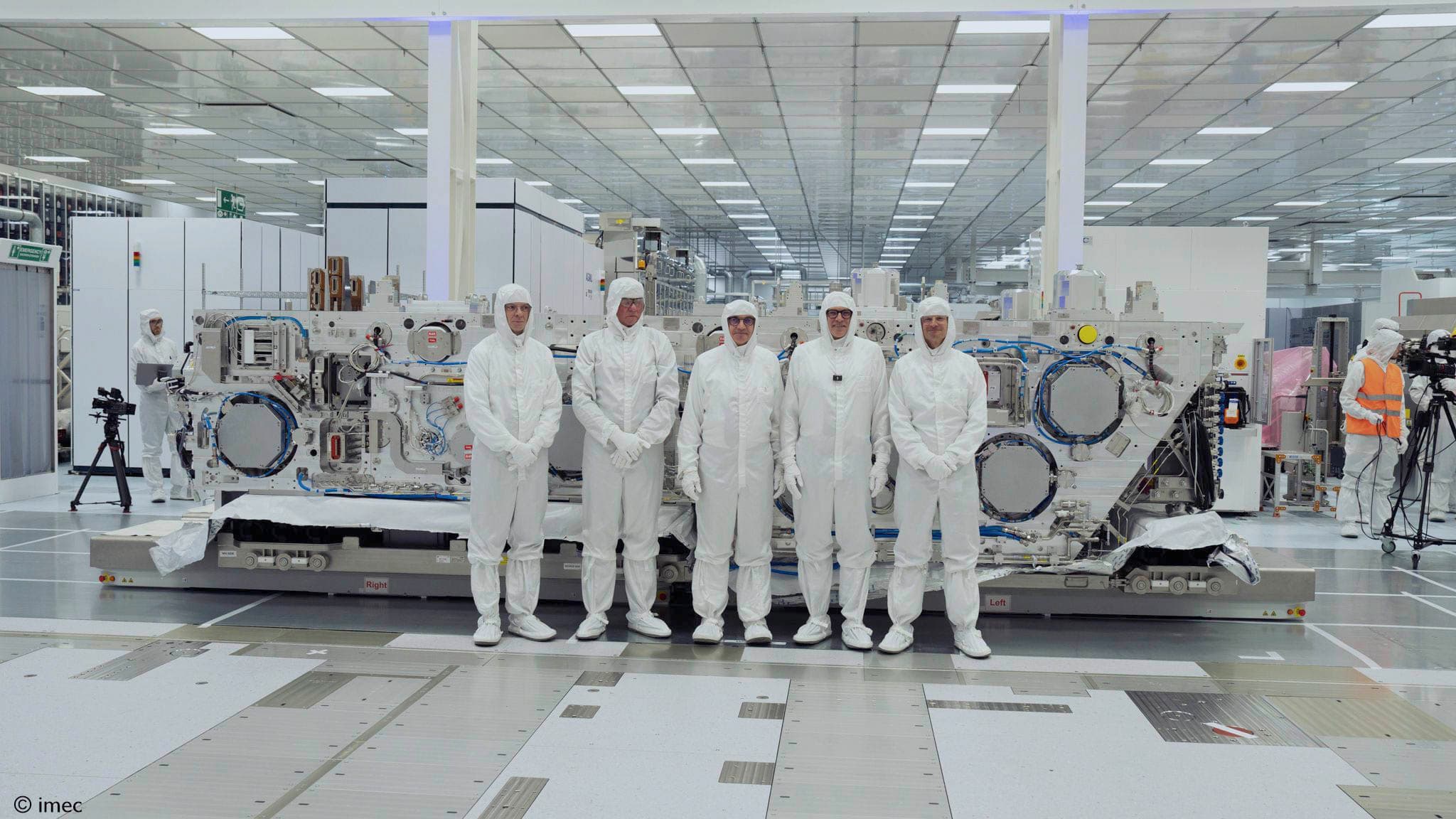
LEUVEN (Belgium), April 25, 2022— This week, at the 2022 SPIE Advanced Lithography and Patterning Conference, imec, a world-leading research and innovation hub in nanoelectronics and digital technologies, presents significant progress in preparing the High-NA patterning ecosystem for the imec-ASML Joint High-NA Lab, which will be centered around the first 0.55NA extreme ultraviolet (EUV) lithography prototype tool. High-NA EUV lithography will be key to advance Moore’s Law beyond 2nm technology generations. Advances are reported in developing patterning and etch processes, in screening new resist and underlayer materials, in improving metrology and in photomask technology.
Luc Van den hove, CEO imec: “Imec is partnering with ASML on High-NA technology as ASML is building its first prototype 0.55NA EUV lithography scanner EXE:5000. High-NA EUV lithography is projected to print the most critical features needed for beyond 2nm logic chips with fewer patterning steps compared to current 0.33NA EUV lithography. It is our role, in tight collaboration with the global patterning ecosystem, to ensure timely availability of advanced resist materials, photomasks, metrology techniques, (anamorphic) imaging strategies, and patterning techniques – to fully benefit from the resolution gain offered by the High-NA EUV lithography scanner. At this year’s SPIE Advanced Lithography Conference, we have 12 contributions in the realm of High-NA EUV lithography, showing that we are well on track to prepare for ecosystem readiness.”
Processes and material optimization for reduced pattern roughness and defectivity
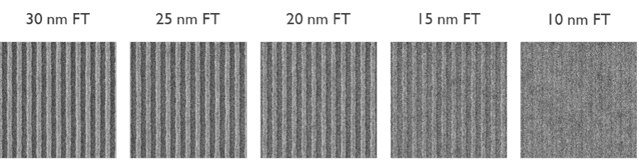
In anticipation of the first High-NA EUV prototyping system, we are pushing the resolution capability of current 0.33NA EUV patterning technologies to predict the performance of thinner resists for printing fine line/spaces and contact holes. In addition to pattern collapse, imec identifies line-edge roughness (LER) as one of the most critical parameters for patterning lines/spaces with thin resist films, and proposes strategies for mitigating pattern roughness (e.g., by tuning illumination and mask conditions). In addition, imec and its material suppliers present the results of screening new resist materials (such as metal-oxide resists) and underlayers with promising pattern transfer capabilities under High-NA conditions. They also propose dedicated patterning and etch schemes aimed at reducing defectivity and stochastic printing failures. (Papers n° 12051-7; 12055-4; 12056-28)
Tailoring the metrology to cope with thin resist films and small feature sizes at high throughput
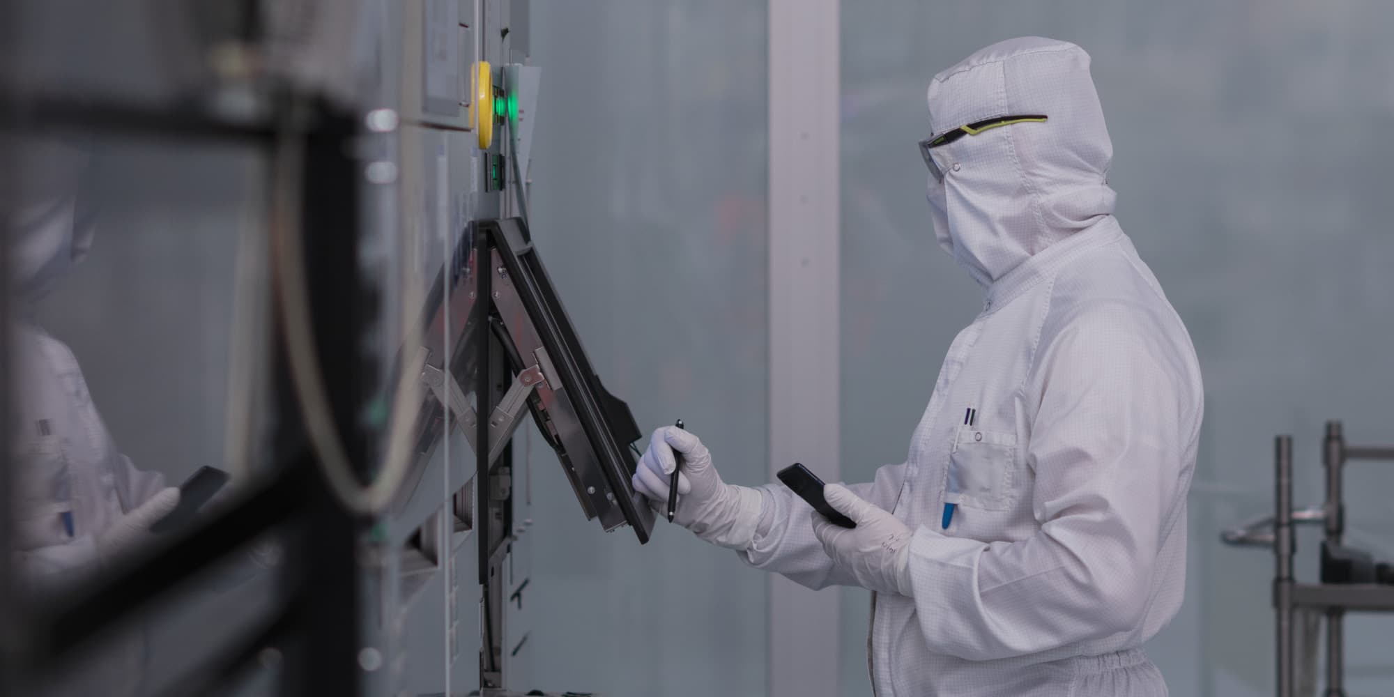
The transition to smaller feature sizes (e.g., 10nm wide lines) and thinner resist films (20nm and below) challenges the metrology in two significant ways. First, metrologists need to cope with a strongly reduced image contrast of CD-SEM tools. Second, the need to image features even smaller than 10nm (taking into account overlay performance, LER and stochastic printing failures) requires metrology tools with improved resolution. Kurt Ronse, Program Director Advanced Patterning imec: “Imec and its partners take several directions to address these challenges. They show that image contrast can be significantly improved by tweaking the operation conditions of existing metrology tools. Image analysis and defect classification are further enhanced by dedicated software, supported by deep learning frameworks (such as deep learning based de-noising). Finally, in close collaboration with its metrology suppliers, imec explores alternative metrology techniques for reliably measuring small features, such as high-throughput scanning probe metrology and low-voltage aberration corrected SEM.” (Papers n° 12053-2; 12053-3; 12053-5; 12053-22; 12053-43; 12053-64)
Addressing High-NA EUV mask specific challenges
Imec has simulated the impact of EUV mask deficiencies (more specifically, mask multilayer ripple and absorber line-edge roughness) upon imaging 22nm pitch lines/spaces. “From this study, it becomes clear that mask imperfections are increasingly impacting the final wafer pattern, indicating that Mask Design Rules need to become tighter,” adds Kurt Ronse. “These findings allow us to identify mask specifications for high-NA EUV lithography. In addition, together with ASML and our material suppliers, we explore novel materials and architectures for the mask absorber, which carries the pattern. In this context, we have for the first time performed exposures to evaluate the impact of using low-n attenuated phase shift masks on imaging both via layers and lines/spaces. Masks with low-n absorber materials as an alternative to currently used Ta-based blanks are shown to improve the mask 3D effects on the wafer, and thus help to increase the high-NA depth of focus.” (Papers n° 12051-37; 12051-51; 12051-56)
About imec
Imec is a world-leading research and innovation center in nanoelectronics and digital technologies. Imec leverages its state-of-the-art R&D infrastructure and its team of more than 5,000 employees and top researchers, for R&D in advanced semiconductor and system scaling, silicon photonics, artificial intelligence, beyond 5G communications and sensing technologies, and in application domains such as health and life sciences, mobility, industry 4.0, agrofood, smart cities, sustainable energy, education, … Imec unites world-industry leaders across the semiconductor value chain, Flanders-based and international tech, pharma, medical and ICT companies, start-ups, and academia and knowledge centers. Imec is headquartered in Leuven (Belgium), and has research sites across Belgium, in the Netherlands and the USA, and offices in China, India, Taiwan and Japan. In 2020, imec's revenue (P&L) totaled 680 million euro.
Further information on imec can be found at www.imec-int.com.
Imec is a registered trademark for the activities of imec International (IMEC International, a legal entity set up under Belgian law as a “stichting van openbaar nut”), imec Belgium (IMEC vzw supported by the Flemish Government), imec the Netherlands (Stichting IMEC Nederland), imec Taiwan (IMEC Taiwan Co.), imec China (IMEC Microelectronics (Shanghai) Co. Ltd.), imec India (IMEC India Private Limited), imec San Francisco (IMEC Inc.) and imec Florida (IMEC USA Nanoelectronics Design Center Inc.).
Discover more

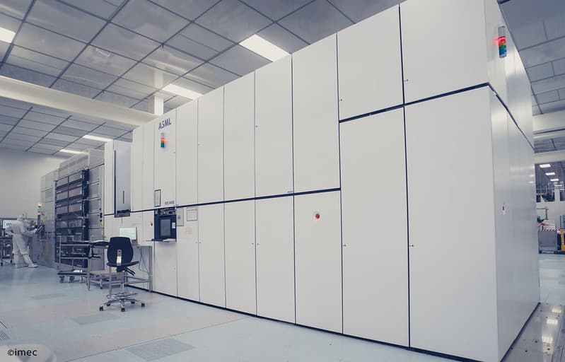
Imec unlocks lever for EUV dose reduction: oxygen injection during metal-oxide resist post-exposure bake emerges as game-changer for throughput
Read more
Imec achieves new milestones in single patterning High NA EUV lithography for both damascene and direct metal etch metallization processes
Read more