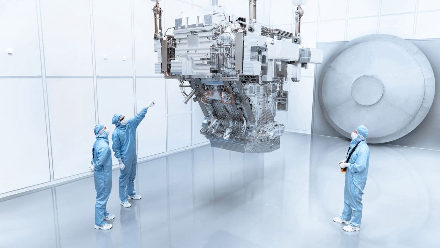
Imec demonstrates readiness of the High-NA EUV patterning ecosystem
Advances in processes, masks and metrology will enable to fully benefit from the resolution gain offered by the first ASML 0.55NA EUV scanner
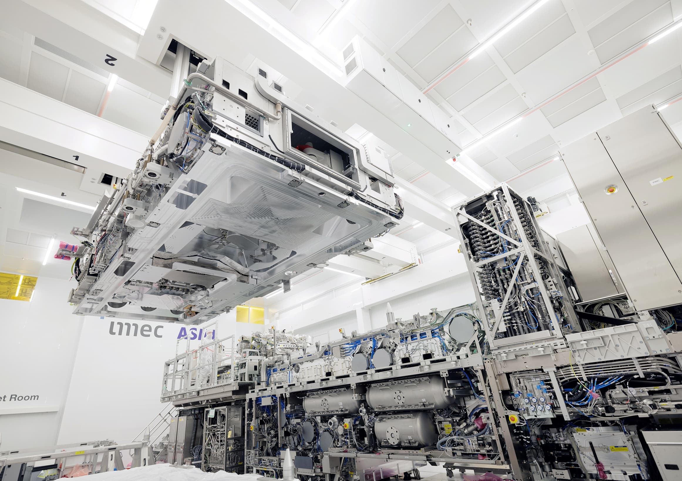
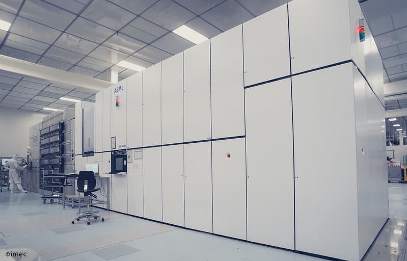
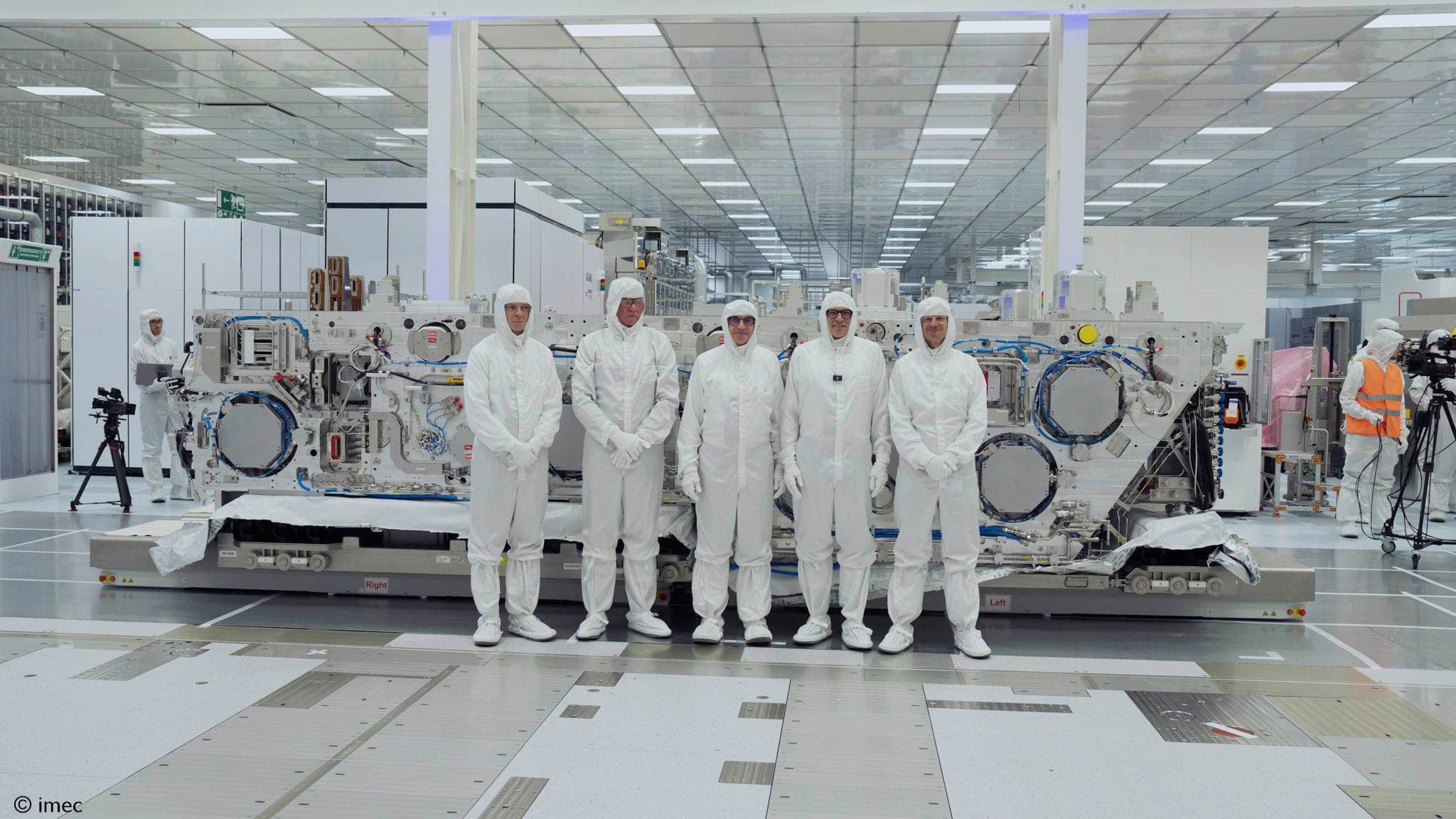
LEUVEN (Belgium), February 26, 2024— This week, at the 2024 Advanced Lithography + Patterning Conference, imec, a world-leading research and innovation hub in nanoelectronics and digital technologies, will present the progress made in EUV processes, masks, and metrology prepared for enabling high-numerical aperture (High-NA) extreme ultraviolet (EUV) lithography. Key achievements are reported on resist and underlayer development, mask enhancement, optical proximity correction (OPC) development, at-resolution field stitching, reduction of stochastic failures, and improved metrology and inspection. With these results, imec demonstrates readiness for transferring the EUV processes into the joint imec-ASML High-NA EUV Lab, built around the first prototype High-NA EUV scanner.
Steven Scheer, senior vice president of Advanced Patterning, Process and Materials at imec: “The first High-NA EUV scanner (TWINSCAN EXE:5000) has been assembled by ASML and the first wafers will be exposed soon. In the next few months, the joint imec-ASML High-NA EUV Lab will be operational, and access will be provided to the High-NA customers. The High-NA EUV lab, with the installed equipment and processes, enables an early start of High-NA EUV learning for the customers before tools are operational in their fabs. It has been imec’s role, in tight collaboration with ASML and our extended supplier network, to ensure timely availability of advanced resist materials, photomasks, metrology techniques, (anamorphic) imaging strategies, and patterning techniques. Readiness of these processes for High-NA enablement is shown in more than 25 papers presented at the 2024 SPIE Advanced Lithography & Patterning Conference.”
Field stitching is a key enabler in High-NA: field stitching is needed because of the anamorphic lens (i.e., a lens with different de-magnification in the x and y directions), resulting in field sizes of half of the conventional scanner field size. Imec will share the latest insights that enable at-resolution stitching based on work done with ASML and our mask shop partners on imec’s NXE:3400C scanner. At-resolution stitching will reduce the need for design changes to cope with the field size reduction.
On the material and process side, it is clear that metal-oxide resists (MORs) are still in the lead for metal line/space patterns. Imec will present the advancements of MOR in terms of EUV dose-to-yield reduction. The selection of the specific underlayer, optimization of the development process, choice of mask absorber, mask bias and mask tonality were leading to a more than 20% dose reduction for lines and spaces, without increased roughness or stochastic failures. Also, tip-to-tip dimensions were not negatively impacted by these dose reduction activities. The dose reduction work continues and is highly appreciated by our chip makers, since it leads to EUV cost reduction due to the higher scanner throughput.
An unexpected result was obtained by using MOR resists with a binary bright field mask for contact hole patterning. A 6% dose reduction with a 30% local CD uniformity (LCDU) improvement was achieved after pattern transfer when comparing to a positive tone chemically amplified resist (CAR) and a binary dark field mask transferred in the same stack. A remaining concern of bright field masks for contact holes is the mask quality and defectivity. This will need careful investigation to make MOR an option for contact holes. Until then, positive tone CAR resists with dark field masks will be the leading candidates for contact and via patterning in High-NA EUV.
High-NA also requires improvements in metrology and inspection, giving the higher resolution (by the high NA) and thinner films (by the reduced depth of focus (DOF)). Imec will present new results on e-beam and deep-UV (DUV) inspection, showing that new best-known methods (BKMs) are in place to find High-NA-relevant stochastic patterning failures, such as hexagonal contact holes. In addition, several machine learning techniques (based on denoising SEM micrographs) will be proposed to facilitate the small defect inspection and classification.
Finally, imaging improvements through source-mask optimizations and anamorphic mask OPC (considering the need for stitching) will be presented by imec and partners.
About imec
Imec is a world-leading research and innovation center in nanoelectronics and digital technologies. Imec leverages its state-of-the-art R&D infrastructure and its team of more than 5,500 employees and top researchers, for R&D in advanced semiconductor and system scaling, silicon photonics, artificial intelligence, beyond 5G communications and sensing technologies, and in application domains such as health and life sciences, mobility, industry 4.0, agrofood, smart cities, sustainable energy, education, … Imec unites world-industry leaders across the semiconductor value chain, Flanders-based and international tech, pharma, medical and ICT companies, start-ups, and academia and knowledge centers. Imec is headquartered in Leuven (Belgium), and has research sites across Belgium, in the Netherlands and the USA, and representation in 3 continents. In 2022, imec's revenue (P&L) totaled 846 million euro.
Further information on imec can be found at www.imec-int.com.
Imec is a registered trademark for the activities of imec International (IMEC International, a legal entity set up under Belgian law as a “stichting van openbaar nut”), imec Belgium (IMEC vzw supported by the Flemish Government), imec the Netherlands (Stichting IMEC Nederland), imec Taiwan (IMEC Taiwan Co.), imec India (IMEC India Private Limited), imec San Francisco (IMEC Inc.) and imec Florida (IMEC USA Nanoelectronics Design Center Inc.).
Discover more
Imec unlocks lever for EUV dose reduction: oxygen injection during metal-oxide resist post-exposure bake emerges as game-changer for throughput
Read more
Imec achieves new milestones in single patterning High NA EUV lithography for both damascene and direct metal etch metallization processes
Read more