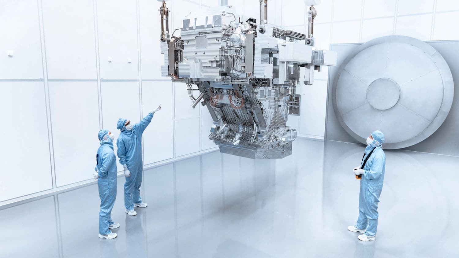
Imec demonstrates CNT pellicle utilization on EUV scanner
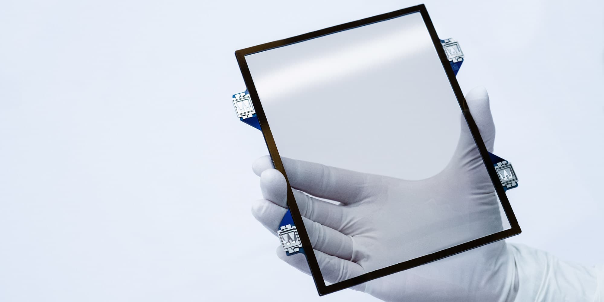
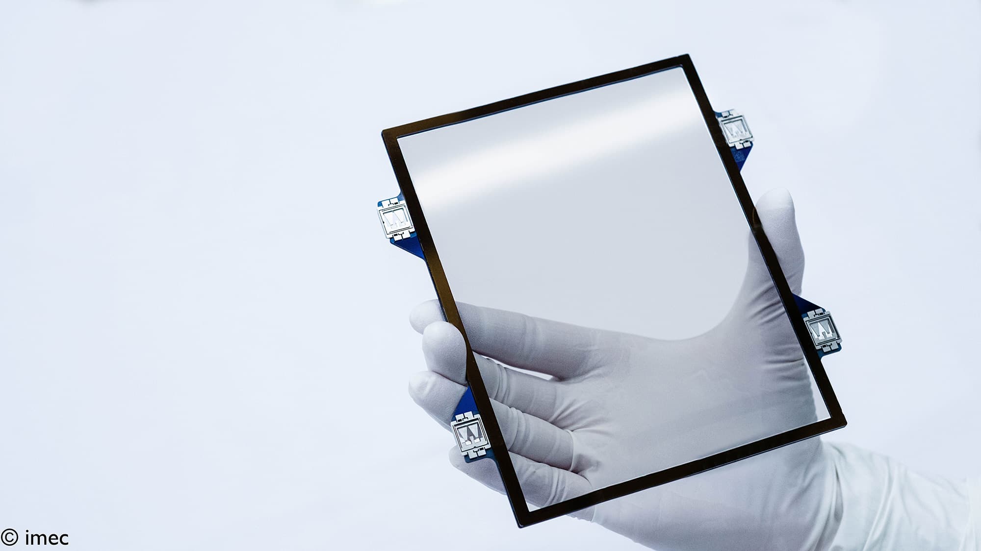
LEUVEN (Belgium) October 6, 2020 — Imec, a world-leading research and innovation hub in nanoelectronics and digital technologies, announced today promising results in extreme ultraviolet (EUV) reticle protection. Multiple CNT-based pellicles were mounted on reticles and exposed in the NXE:3300 EUV scanner at imec, demonstrating the successful fabrication and scanner handling of full-field CNT-based pellicles. The tested pellicles had a single-pass EUV transmission up to 97%. The impact on imaging was found to be low and correctable based on critical dimension (CD), dose, and transmission measurements.
A pellicle is a membrane used to protect the photomask from contamination during high-volume semiconductor manufacturing. It is mounted a few millimeters above the surface of the photomask so that if particles land on the pellicle, they will be too far out of focus to print. Developing such an EUV pellicle is very challenging, since 13.5nm light is absorbed by most materials. In addition, stringent thermal, chemical, and mechanical requirements must be achieved. Such highly transparent pellicle is critical to enable high yield and throughput in advanced semiconductor manufacturing.
Imec has leveraged partners in the semiconductor industry, materials companies and fundamental research to develop an innovative EUV pellicle design with potential to survive scanner powers beyond 600 Watts
“Imec has leveraged partners in the semiconductor industry, materials companies and fundamental research to develop an innovative EUV pellicle design with potential to survive scanner powers beyond 600 Watts,” said Emily Gallagher, principal member of technical staff at imec. “We have seen tremendous progress in carbon nanotube membrane development in the past year and, based on strong collaborations with our partners, are confident it will result in a high-performance pellicle solution in the near future.”
CNTs are one-atom-thick carbon sheets rolled into tubes. The CNTs can be single-, double- or multi-walled and can vary in diameter and in length. These engineered CNTs can be arranged in different configurations to form membranes of different densities. Since 2015, imec has been working with selected CNT suppliers (Canatu Oy and Lintec of America, Inc., Nano-Science & Technology Center) to develop membranes that meet the EUV pellicle targets for properties like transmittance, thermal durability, permeability, and strength and to enable the imaging results reported today. Future work will focus on achieving acceptable lifetimes for high volume manufacturing of these pellicles in scanners.
About imec
Imec is a world-leading research and innovation hub in nanoelectronics and digital technologies. The combination of our widely acclaimed leadership in microchip technology and profound software and ICT expertise is what makes us unique. By leveraging our world-class infrastructure and local and global ecosystem of partners across a multitude of industries, we create groundbreaking innovation in application domains such as healthcare, smart cities and mobility, logistics and manufacturing, energy and education.
As a trusted partner for companies, start-ups and universities we bring together more than 4,000 brilliant minds from almost 100 nationalities. Imec is headquartered in Leuven, Belgium and has distributed R&D groups at a number of Flemish universities, in the Netherlands, Taiwan, USA, and offices in China, India and Japan. In 2019, imec's revenue (P&L) totaled 640 million euro. Further information on imec can be found at www.imec-int.com.
Imec is a registered trademark for the activities of IMEC International (a legal entity set up under Belgian law as a "stichting van openbaar nut”), imec Belgium (IMEC vzw supported by the Government of Flanders), imec the Netherlands (Stichting IMEC Nederland, part of Holst Centre and OnePlanet, supported by the Dutch Government), imec Taiwan (IMEC Taiwan Co.), imec China (IMEC Microelectronics (Shanghai) Co. Ltd.), imec India (Imec India Private Limited) and imec Florida (IMEC USA nanoelectronics design center).
Discover more

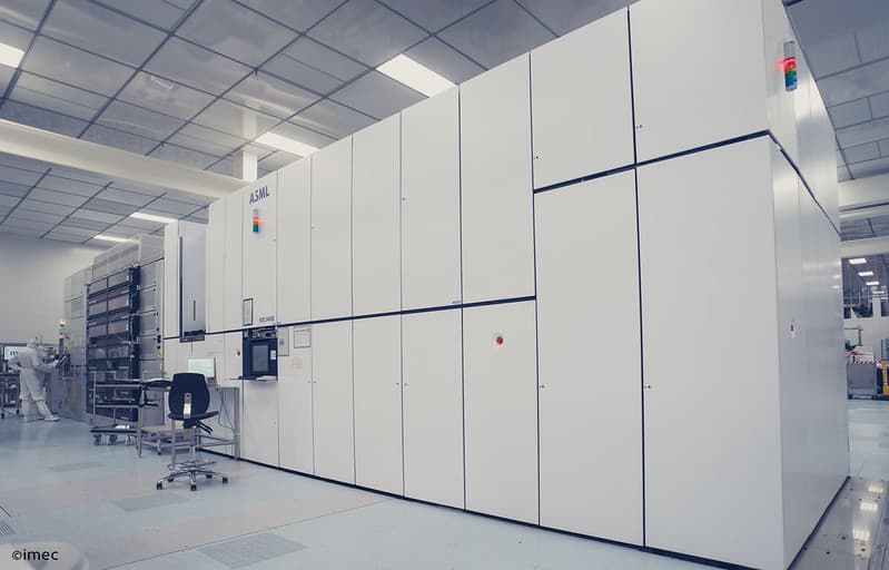
Imec unlocks lever for EUV dose reduction: oxygen injection during metal-oxide resist post-exposure bake emerges as game-changer for throughput
Read more
Imec achieves new milestones in single patterning High NA EUV lithography for both damascene and direct metal etch metallization processes
Read more