First full wafer-scale fabrication of electrically-pumped GaAs-based nano-ridge lasers on 300 mm silicon wafers
Imec achieves breakthrough in silicon photonics, paving the way for cost-effective and high-performance optical devices.
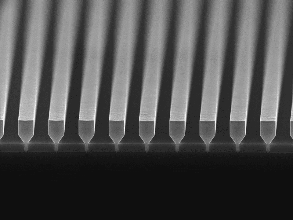
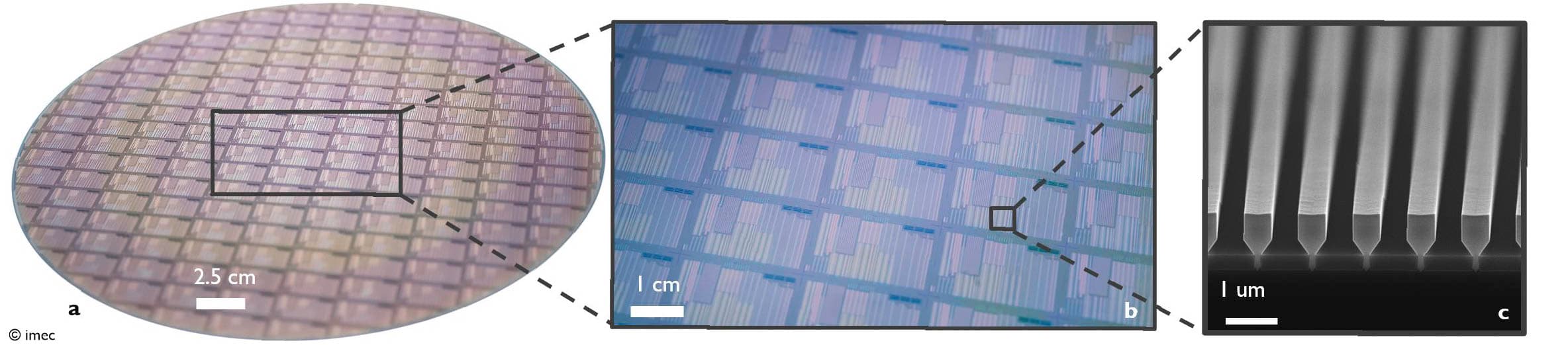
LEUVEN (Belgium), JANUARY 9, 2025— Imec, a world-leading research and innovation hub in nanoelectronics and digital technologies, has announced a significant milestone in silicon photonics with the successful demonstration of electrically-driven GaAs-based multi-quantum-well nano-ridge laser diodes fully, monolithically fabricated on 300 mm silicon wafers in its CMOS pilot prototyping line. Achieving room-temperature continuous-wave lasing with threshold currents as low as 5 mA and output powers exceeding 1 mW, the results, detailed in last week’s Nature publication, demonstrate the potential of direct epitaxial growth of high-quality III-V materials on silicon. This breakthrough provides a pathway to the development of cost-effective, high-performance optical devices for applications in data communications, machine learning and artificial intelligence.
The lack of highly scalable, native CMOS-integrated light sources has been a major roadblock for the widespread adoption of silicon photonics. Hybrid or heterogeneous integration solutions, such as flip-chip, micro-transfer printing or die-to-wafer bonding, involve complex bonding processes or the need for expensive III-V substrates which are often discarded after processing. This not only increases costs but also raises concerns about sustainability and resource efficiency. For that reason, the direct epitaxial growth of high-quality III-V optical gain materials selectively on large-size silicon photonics wafers remains a highly sought-after objective.
The large mismatch in crystal lattice parameters and thermal expansion coefficients between III-V and Si materials inevitably initiates the formation of crystal misfit defects, which are known to deteriorate laser performance and reliability. Selective-area growth (SAG) combined with aspect-ratio trapping (ART) significantly reduces defects in III-V materials integrated on silicon by confining misfit dislocations within narrow trenches etched in a dielectric mask.
“Over the past years, imec has pioneered nano-ridge engineering, a technique that builds on SAG and ART to grow low-defectivity III-V nano-ridges outside the trenches. This approach not only further reduces defects but also enables precise control over material dimensions and composition. Our optimized nano-ridge structures typically feature threading dislocation densities well below 105 cm-2. Now, imec exploited the III-V nano-ridge engineering concept to demonstrate the first full wafer-scale fabrication of electrically pumped GaAs-based lasers on standard 300 mm silicon wafers, entirely within a CMOS pilot manufacturing line,” says Bernardette Kunert, scientific director at imec.
Leveraging the low-defectivity GaAs nano-ridge structures, the lasers integrate InGaAs multiple quantum wells (MQWs) as the optical gain region, embedded in an in-situ doped p-i-n diode and passivated with an InGaP capping layer. Achieving room-temperature, continuous-wave operation with electrical injection is a major advancement, overcoming challenges in current delivery and interface engineering. The devices show lasing at ~1020 nm with threshold currents as low as 5 mA, slope efficiencies up to 0.5 W/A, and optical powers reaching 1.75 mW, showcasing a scalable pathway for high-performance silicon-integrated light sources.
“The cost-effective integration of high-quality III-V gain materials on large-diameter Si wafers is a key enabler for next-generation silicon photonics applications. These exciting nano-ridge laser results represent a significant milestone in using direct epitaxial growth for monolithic III-V integration. This project is part of a larger pathfinding mission at imec to advance III-V integration processes towards higher technological readiness, from flip-chip and transfer-printing hybrid techniques in the near term, over heterogeneous wafer- and die-bonding technologies and eventually direct epitaxial growth in the longer term,” states Joris Van Campenhout, fellow silicon photonics and director of the industry-affiliation R&D program on Optical I/O at imec.
About imec
Imec is a world-leading research and innovation center in nanoelectronics and digital technologies. Imec leverages its state-of-the-art R&D infrastructure and its team of more than 5,500 employees and top researchers, for R&D in advanced semiconductor and system scaling, silicon photonics, artificial intelligence, beyond 5G communications and sensing technologies, and in application domains such as health and life sciences, mobility, industry 4.0, agrofood, smart cities, sustainable energy, education, … Imec unites world-industry leaders across the semiconductor value chain, Flanders-based and international tech, pharma, medical and ICT companies, start-ups, and academia and knowledge centers. Imec is headquartered in Leuven (Belgium), and has research sites across Belgium, in the Netherlands, the UK and the USA, and representation in 3 continents. In 2023, imec's revenue (P&L) totaled 941 million euro.
Further information on imec can be found at www.imec-int.com.
Imec is a registered trademark for the activities of imec International and its affiliated entities.
Discover more

Imec unveils 7‑bit, 175GS/s massively time-interleaved slope-ADC – pairing record-small footprint and low conversion energy with top sampling speed
Read more



Veeco and imec develop 300mm-compatible process to enable integration of barium titanate on silicon photonics
Read more
A double world-first: integrating lithium niobate and lithium tantalate modulators on silicon photonics through micro-transfer printing
Read more

Imec debuts a beyond-110GHz C-band GeSi electro-absorption modulator (EAM) on its 300mm silicon photonics platform
Read more