Through the EU SPEAR project, imec offers training on SOT-MRAM: emerging memory for microcontrollers and embedded systems
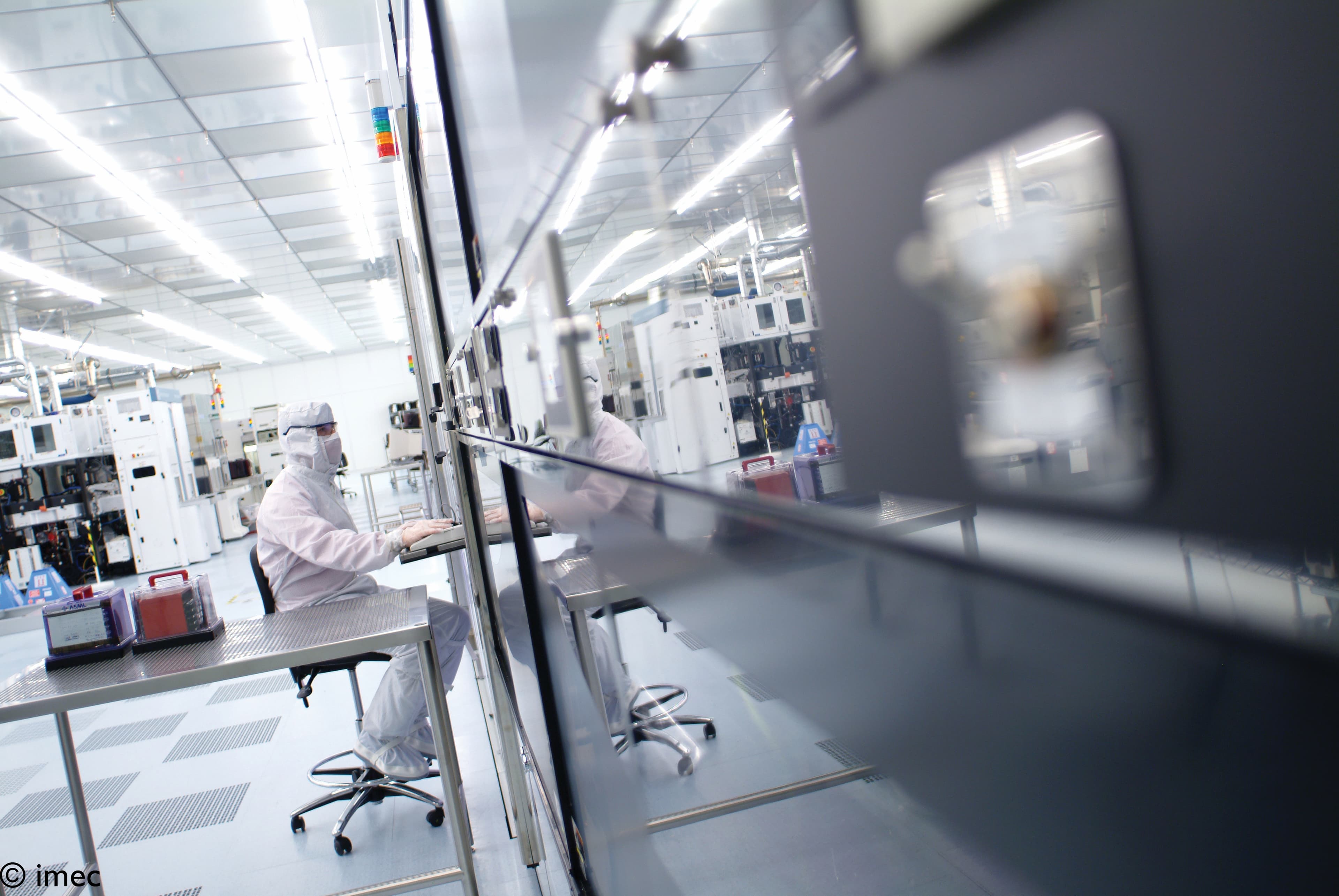
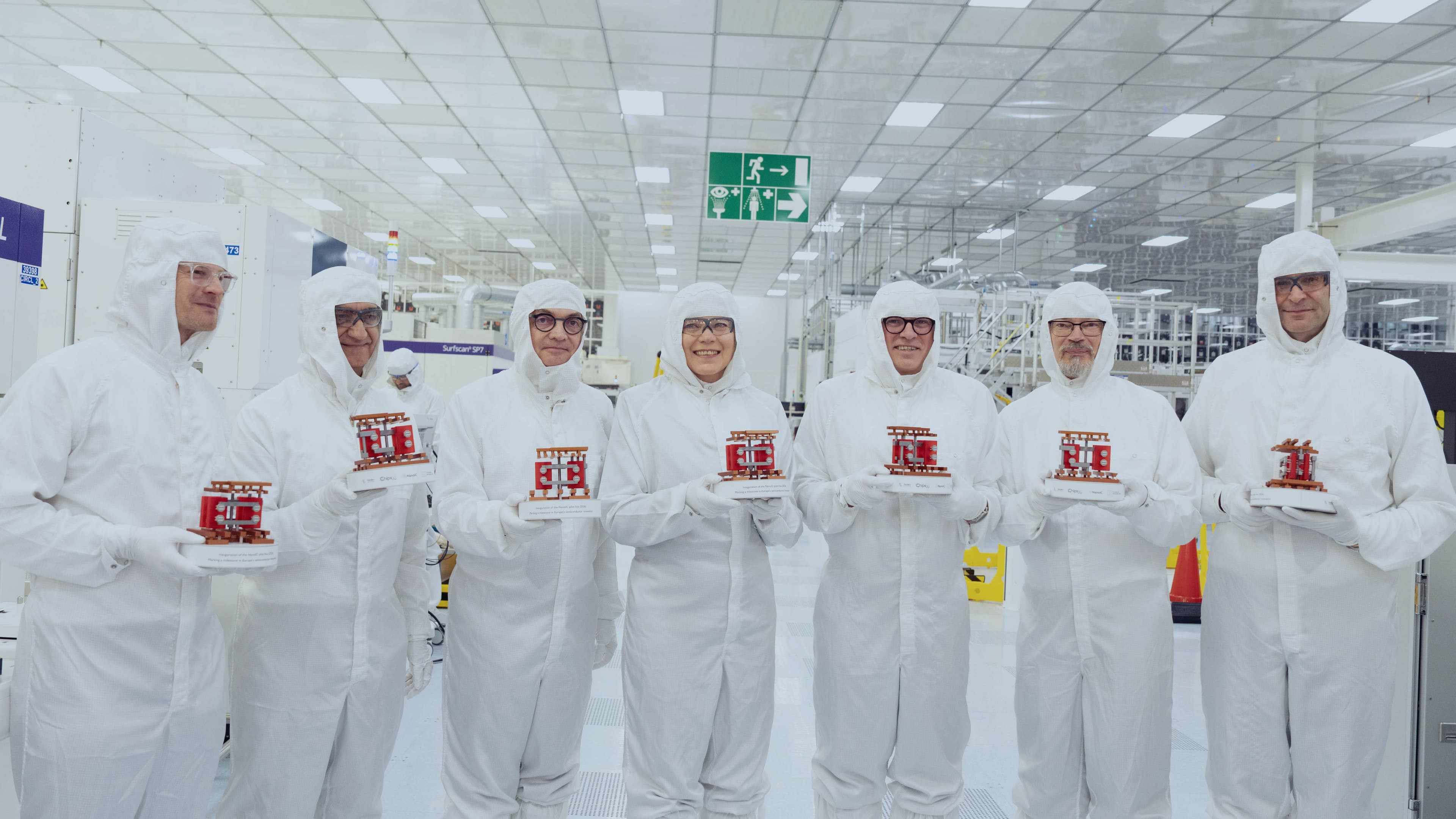
From October 3 to 5, imec organized a hybrid (offline/online) training on SOT-MRAM technology for memory, from fundamentals to materials to integration and circuit design challenges.
The content remains available through imec.academy and is suitable for any profile that relates to magnetics, emerging memories and magnetic memories in general and is suitable both to master level students up to trained experts that want to have a deep insight in upcoming technologies.

From October 3 to 5, imec organized a hybrid (offline/online) training on SOT-MRAM technology for memory, from fundamentals to materials to integration and circuit design challenges. Setup in the framework of the EU-funded SPEAR project and supported by imec academy, the content is relevant for any profile that relates to magnetics, emerging memories, and magnetic memories in general, and is relevant for master-level students up to trained experts that want deep insight in upcoming technologies.
These trainings are important because fundamental knowledge of the physics and scientific phenomena behind SOT-MRAM has only been relatively recently discovered while it’s already at the basis of more applied R&D towards specific implementations in semiconductor memories. More precisely, the first papers on the fundamentals behind SOT-MRAM only date back to around 2012 and it is already considered one of the most promising candidates for future generations of memory in microcontrollers and embedded devices. The SPEAR project is an example of the type of initiatives that can ensure sufficient effort is put into furthering the fundamental knowledge about relatively young scientific topics while ensuring that the explorations align with the needs of the already ongoing industrial R&D.
Best practice for EU Chips Act
Within SPEAR, 15 PhDs have been selected and recruited on a variety of emerging technologies, two of which are being hosted by imec on the topic of SOT-MRAM. For these 15 high potentials, a dedicated development trajectory is being designed with a combination of trainings on technical topics and on other relevant skills. The technical trainings are being opened for a wider audience. The current training is the second out of five and can count on the support of imec academy for the organization of the training and in the capitalization for later use in similar contexts. It is a concrete illustration of some elements of the skills-development strategy put forward by the EU Chips Act. Within this European context, several emerging technologies are being considered important differentiators in the aim for an increased global competitiveness. In the case of memory technologies, each of Europe’s three main Research and Technology Organizations (RTO) has chosen a specific emerging technology to focus on. For Fraunhofer, this is ferroelectric RAM, for CEA-LETI it is phase-change memory and imec focuses on MRAM. It's a great example of how teaming up at the European level can allow us to share tasks and make progress on multiple levels by optimally leveraging each other’s knowledge and capabilities.
The potential of SOT-MRAM
The biggest added value and application potential of SOT-MRAM is believed to be situated in the domain of microcontrollers and embedded systems, and more specifically, for technology nodes of 14nm and beyond.
Up until the 28nm node, the needs for non-volatile memories in this market was largely catered to a specific flavor of NAND Flash memory. Yet, the heterogeneous processing that was needed to integrate this working memory on top of logic became too complex and unsustainable in terms of cost. New non-volatile memory concepts such as resistive memory, phase-change memory and STT MRAM, therefore came around the corner because of their more compatible process flow. With the first two proving their value in the 22 and 18nm nodes, STT MRAM is currently the one of these few candidates that made it into the 14nm production node. Partly because MRAM can be switched through advanced transistors (operating at 0,7V and below), while other emerging memory technologies would need a specific transistor to provide a higher voltage.
SOT-MRAM differentiates itself by its fast-switching potential. This would allow it to match the clock speeds of the CPU on top of which it is being embedded and even to take on the additional role of working memory.
Within the MRAM domain, STT is proving its value in current technology nodes, but has some intrinsic characteristics that prevent it from being used as a real cache memory. For example, it is a two-pillar device that achieves switching by passing a high current through very thin dielectric layers, limiting its endurance. Here, SOT-MRAM holds the advantage for future technology nodes. Being a three-terminal device, it decouples the read and write paths and thereby avoids large currents running through critical layers. Other than STT, this allows SOT to reach the theoretically feasible switching speeds of MRAM. For completeness, it must be stated that SOT MRAM is somewhat bulkier compared to STT-MRAM devices and therefore introduces another specific set of challenges in terms of density and footprint. But for the long-term scaling, it is by far the best candidate. Initiatives like the training within the EU-SPEAR project are therefore invaluable for the long-term future of the entire domain of embedded systems.
Authors

Sebastien Couet
Sebastien Couet received his PhD in physics from the University of Hamburg, Germany, in 2008. From 2009 to 2014, he was a postdoctoral fellow at the Katholieke Universiteit Leuven, Belgium, where he specialized in the interface physics of magnetic/oxide heterostructures. In 2014, he joined imec, Leuven, where he is currently the program director for magnetics. In this role, he oversees the development of the various MRAM-based memory concepts for embedded and standalone applications and other exploratory magnetic device concepts.