The vertical nanowire FET: enabler of highly dense SRAMs
Gate-all-around nanowire field effect transistors (FETs) in a vertical configuration bring many opportunities, such as the 'super-scaling' of SRAM memory cells.

Intro
Gate-all-around nanowire field effect transistors (FETs) in a vertical configuration can be considered strong candidates to extend today’s CMOS technology to its ultimate scaling limits. With an excellent performance/area ratio, they seem particularly attractive for making highly dense static random access memory (SRAM) cells. Moreover, when used to building those SRAM cells, vertical nanowire FETs may play a key role in hybrid scaling – an emerging scaling approach that integrates multiple transistor architectures in one system-on-chip.
In this article, Nadine Collaert (distinguished member of technical staff at imec), Anabela Veloso (principal member of technical staff at imec) and Trong Huynh-Bao (R&D engineer at imec) highlight the opportunities brought by vertical nanowire FETs. They also discuss the possible device integration routes and talk about the ‘super-scaling’ of SRAM cells.
Moving towards hybrid scaling
Traditional device scaling has been one of the cornerstones of the semiconductor industry ever since Gordon Moore presented ‘Moore’s Law’ back in 1965. More recently, however, another trend has started to emerge on the technology roadmap: hybrid scaling – also referred to as hybridized scaling, heterogeneous scaling or heterogeneous integration.
"The fundamental difference with traditional device scaling is that hybrid scaling features no preferred device architecture that makes up a system."
Instead, multiple device technologies are applied to create different subsystems of a system-on-chip, depending on their function in the system. For example, magnetoresistive random access memory (MRAM) could be used for embedded cache memory, aggressively scaled FinFETs for the highest performance CPU cores, and spin logic devices for ultra-low-power functions. In the context of future hybrid scaling, the vertical nanowire field effect transistor (FET) has the potential to become an important player as well. As recently shown at imec, it is a promising technology for enabling highly dense static random access memory (SRAM) cells.
The vertical nanowire FET
Gate-all-around (GAA) nanowire/nanosheet FETs are, to a certain extent, a natural evolution of today’s FinFET technology. In these devices, the gate is fully wrapped around the thin conduction channel (the nanowire) of the transistor, allowing superior short channel electrostatic (SCE) control, as required for more advanced technology nodes. The technology also promises further density scaling, which becomes increasingly problematic because of challenges in gate pitch scaling.
Nanowire FETs can be implemented in a lateral or a vertical configuration. That said, devices in a lateral configuration still use conventional 2D layouts, and hence their scaling into advanced nodes will eventually hit physical limits, similarly to FinFETs. For example, the space available for gate and contact placement will become too small. Moreover, in the back-end-of-line, too many metal lines in increasingly narrow spaces will give rise to interconnect routing congestion.
And that’s where the vertical GAA nanowire FETs come into play. With these devices, we move from a 2D to a 3D layout configuration, wherein the gate length is defined vertically. Such a disruptive innovation requires early process-design co-optimization, but it also leads to new opportunities.
A key advantage is that, in a vertical configuration, the gate length is not restricted by the device footprint.
This means that the gate length can be more relaxed without consuming a larger area on the wafer. It also allows some relaxation in the nanowire diameter while preserving control over the short channel effects. Both are beneficial for variability considerations.
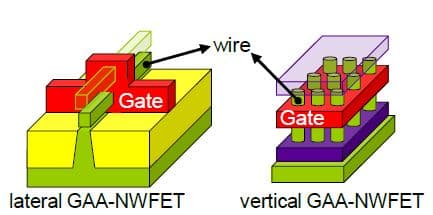
"Furthermore, relaxing the nanowire size can be advantageous for high-mobility channel devices that use germanium (Ge) or III-V materials as an alternative to Si."
These high-mobility channel materials hold the promise to reduce the power consumption by decreasing the operating voltages while maintaining and even increasing the performance. However, for smaller nanowire diameters, several theoretical studies predict mobility degradation which would offset the benefits of using high-mobility materials. This problem could be mitigated by using nanowires in a vertical configuration, which allows for more relaxed nanowire dimensions.
Also in terms of power consumption and RC parasitics, the vertical nanowire shows considerable potential.
"Imec has made a comparative analysis between (triple gate) FinFETs, lateral nanowire FETs and vertical nanowire FETs."
Firstly, for projected 5nm technology node dimensions, vertical nanowire FETs exhibit lower parasitic capacitance and resistance (RC) values than the other two architectures. For lateral nanowire FETs, by vertically stacking lateral wires, an enhanced drive current can be achieved, but this will come at the cost of increased RC parasitics. Secondly, calculations show that vertical nanowire FETs clearly outperform the other devices in terms of energy consumption. The latter is particularly critical as low power consumption has become an important asset, especially given the growing trend for increasingly more portable and wearable applications.
Enabling dense SRAM cells
Relaxation in the gate length is also an important knob for optimizing process variability, which is especially critical in scaled SRAMs. SRAM cells are typically composed of 6 transistors. To achieve better performing and more stable SRAM cells, a well-known engineering knob is to increase the gate length of one or more of these transistors. But when the SRAM cell is based on lateral nanowire transistors, increasing the gate length means increasing the cell’s footprint on the wafer.
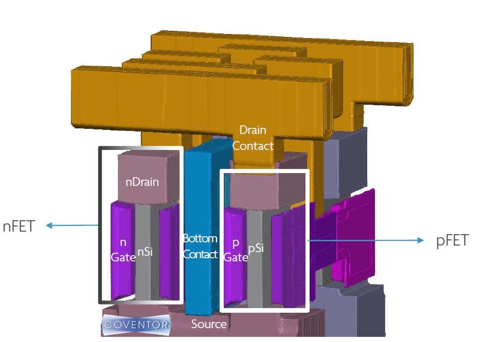
With vertical nanowire FETs, the gate length can be relaxed for a more optimal performance and improved stability without consuming more SRAM cell area.
The excellent performance/area ratio also makes for better SRAM scaling. For projected 5nm node design rules, imec has calculated a 30% area reduction for 6-transistor (6T) SRAM bit-cells built with vertical nanowire FETs instead of lateral nanowire FETs. In addition, these highly scaled SRAM cells show improved read and write stability, lower minimum operating voltages and lower standby leakage values.
Device integration: the channel-first approach
From device integration perspective, a simpler route to make vertical nanowire devices (with one or more gate levels) would leverage a channel-last approach – a route that is commonly followed for integrating nanowire structures in memory applications. In a channel-last approach, a hole is etched through a layer stack. Next, this hole is filled with the material of choice by selective epitaxial growth, followed by a chemical mechanical polish (CMP). But for logic and SRAM applications, this route has two main drawbacks: the growth of high-quality (defect-free) channels and the doping of the nanowires – which is required for junction formation in logic applications – are difficult to achieve.
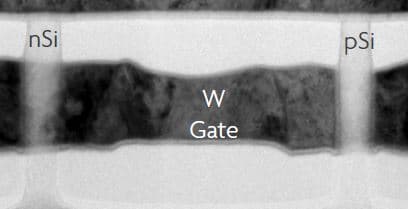
"Therefore, imec has so far pursued a channel-first approach, thus allowing better quality channels and more flexibility in the choice of materials (e.g. Si or high-mobility channel materials), while holding more options for channel doping."
In this channel-first route, nanowire pillars are formed and doping is introduced prior to other processing steps (such as isolation, gate and contact formation). Si nanowire doping is performed by growing up to three stacked layers for one wire, each with different dopant concentrations for a given transistor type (nMOS/pMOS). For extra simplicity, junction-less type of devices could be considered for the fabrication of these vertical nanowire FETs as they do not require junctions.
Outlook: vertically stacked VNWFETs, the path to super-scaled SRAM cells
Integrating nanowires in a vertical architecture is a promising approach for making highly dense SRAM cells.
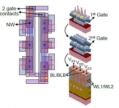
In the longer term, we can go a step further and even stack these vertical transistors on top of each other.
Imec has explored such a novel SRAM cell design, where a 6-transistor SRAM cell is stacked on top of another 6-transistor SRAM cell. Stacking is done in such a way that two stacked transistors are of the same doping type. An interconnect layer is defined vertically in-between the two transistor gate levels. With this design, simulations show a 39% area reduction (per bit) with respect to SRAM designs that have only one level of vertical nanowire FETs. Importantly, no performance degradation is expected from this new, highly-scaled 3D cell design. In summary, stacking of vertical nanowire devices is a promising path towards high-performance ‘super-scaled’ SRAM cells.
Want to know more?
- Read ‘Vertical nanowire FET integration and device aspects’ by A. Veloso et al., ECS Transactions, 72 (4) 31-42 (2016)
- Read ‘Challenges and opportunities of vertical FET devices using 3D circuit design layout’ by A. Veloso et al., SOI-3D-Subthreshold Microelectronics Technology Unified Conference (S3S), 2016 IEEE
Authors

Anabela Veloso
Anabela Veloso received a 5-years college degree (M.Sc.) in applied physics engineering from the Instituto Superior Técnico (IST)-Technical University of Lisbon, Portugal, in 1996. Until 2001, she worked for her Ph.D. studies on advanced magnetic read heads (Ph.D. degree in 2002 from INESC-IST, Portugal, including an internship at Storage Technology Corporation, Louisville, Colorado, USA in 2000). Since 2001, she has been working at imec, in Leuven, Belgium, where she is a principal engineer. Currently, her main research interests are in the areas of advanced CMOS device physics, characterization and technology, leading the nanowires project from the imec Core CMOS Logic program. She has authored or co-authored more than 200 papers published in peer-reviewed international conference proceedings and technical journals, and she was an IEDM Process and Manufacturing Technology (PMT) committee member in 2014-2015.

Trong Huynh-Bao
Trong Huynh-Bao received an M.Sc. degree from Politecnico di Torino, Italy in 2012 (summa cum laude). In 2017, he obtained a Ph.D. degree with the highest honor from imec, Leuven and Vrije Universiteit Brussel for his research on Design-Technology Co-optimization (DTCO) of vertical gate-all-around transistors for the beyond-5nm CMOS generations. Since 2017, he has been an R&D engineer at imec focusing on different aspects of DTCO for sub-10nm nodes, embedded SRAM, emerging memories, and circuit design enablers for extending Moore’s Law.

Nadine Collaert
Nadine Collaert is program director at imec and responsible for the High-speed analog/RF program. She received an M.S. and Ph.D. degree in electrical engineering from the ESAT Department, KU Leuven, Belgium, in 1995 and 2000, respectively. Since then, she has been involved in the theory, design and technology of FinFET devices, emerging memory devices, transducers for biomedical applications and the heterogeneous integration of new materials with Si.
Discover more



Imec and Diraq demonstrate first coherent operation of eight silicon MOS spin qubits fabricated in a 300mm CMOS-compatible foundry process
Read more


Neural telemetry breakthrough: new chip delivers ten-fold compression while preserving signal integrity
Read more

